Binary adder
- Summary
- Abstract
- Description
- Claims
- Application Information
AI Technical Summary
Problems solved by technology
Method used
Image

Examples
second embodiment
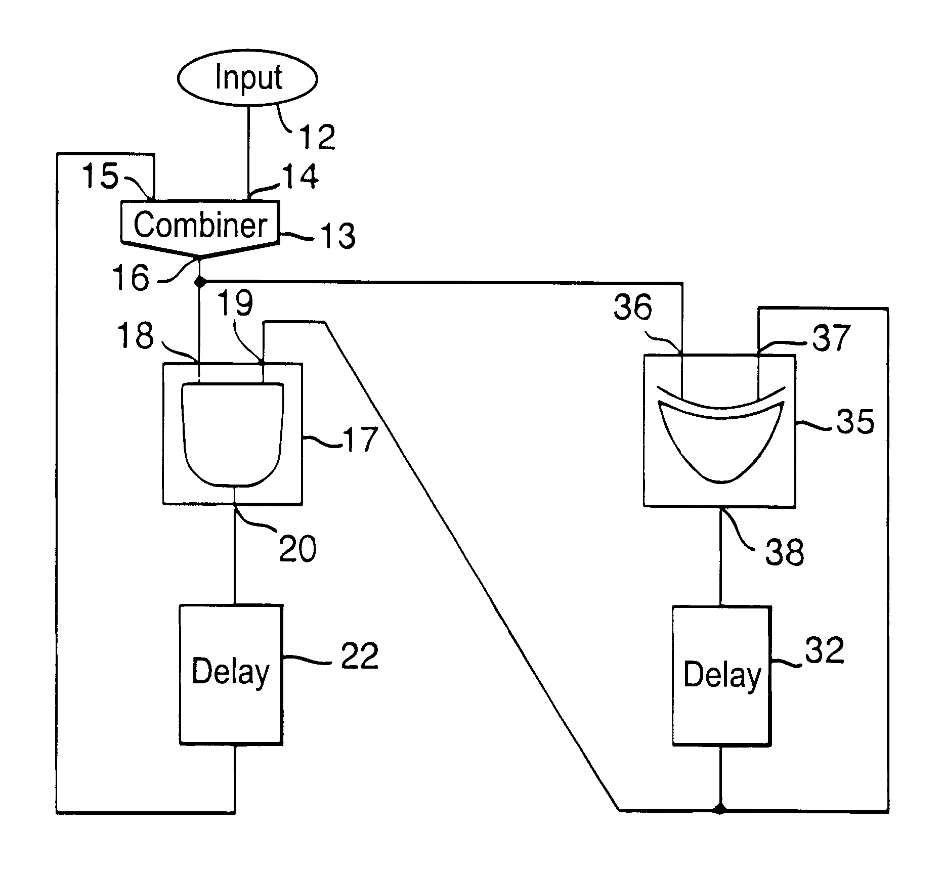
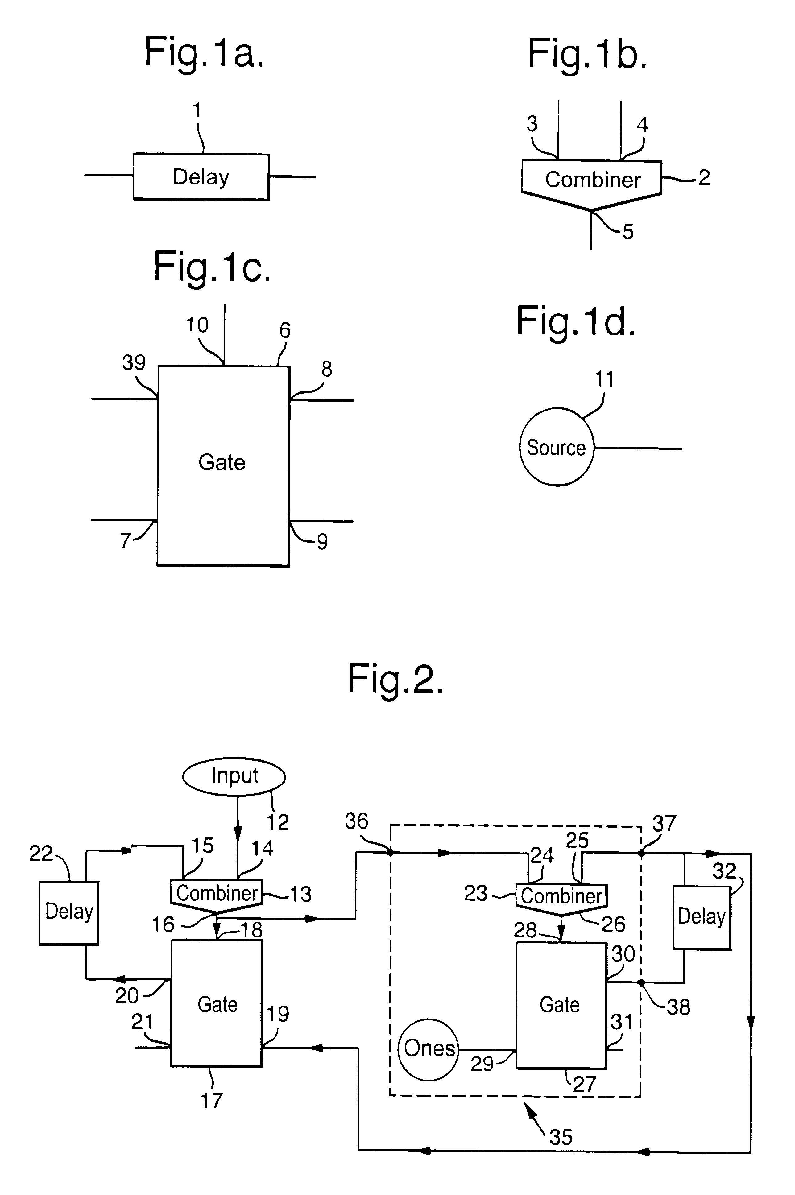
the present invention is shown in schematic form in FIG. 8 which shows a schematic representation of the configuration of the logic gates used for this alternative design. Components in FIG. 8 identical to those in FIG. 4 are indicted by equivalent reference numerals except increased by 100.
As shown in FIG. 8, the adder comprises an AND gate 117 and an XOR gate 135. The AND gate output 120 is coupled via a delay line 122, that introduces a L+1 bit slot delay, to the first AND gate input 118 and the first XOR gate input 136. The XOR gate output 138 is coupled via a delay line 122, that introduces an L bit slot delay, to the second AND gate input 119 and the second XOR gate input 137. An input 112, which supplies the words to be added is coupled to the first AND gate input 118 and the first XOR gate input 136.
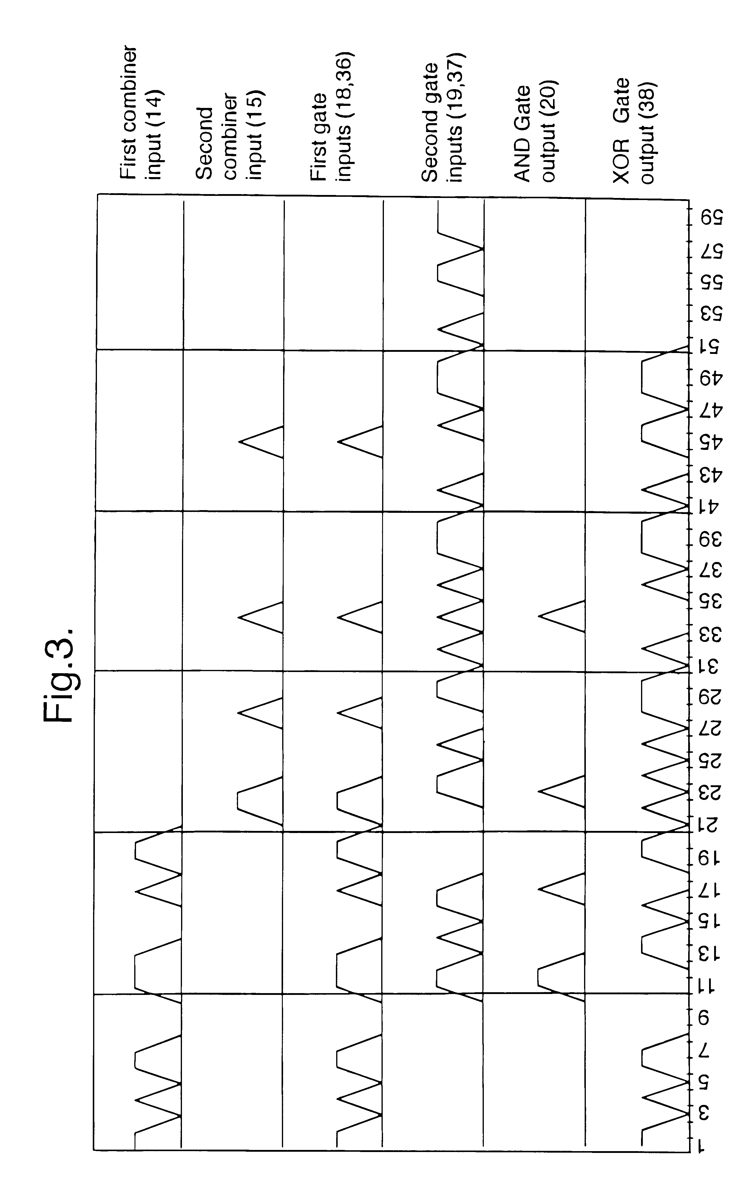
Comparison of FIGS. 4 and 8 shows that FIG. 8 is similar to the apparatus of FIG. 4 with the optical combiner 13 removed. Examination of the optical pulses in FIG. 3 shows that t...
PUM
 Abstract
Description
Claims
Application Information
 - R&D Engineer
- R&D Manager
- IP Professional
- Industry Leading Data Capabilities
- Powerful AI technology
- Patent DNA Extraction
Browse by: Latest US Patents, China's latest patents, Technical Efficacy Thesaurus, Application Domain, Technology Topic.
© 2024 PatSnap. All rights reserved.Legal|Privacy policy|Modern Slavery Act Transparency Statement|Sitemap