Eit-based photonic logic gate

a logic gate and photonic technology, applied in logic circuits, pulse techniques, instruments, etc., can solve the problems of fixed structure and inability to change the refractive index of the ga

Active Publication Date: 2013-01-17
CHUNG HUA UNIVERSITY
View PDF0 Cites 2 Cited by
  • Summary
  • Abstract
  • Description
  • Claims
  • Application Information

AI Technical Summary

Benefits of technology

[0010]For remedying the shortcomings of the prior art, the present invention provides an EIT-based photonic logic gate that includes at least N EIT-based stack layers periodically arranged. Each of the EIT-based stack layers has a photonic crystal layer and an EIT material layer. The photonic crystal layer is made of a material having a positive, zero or negative refractive index, and the photonic crystal layer has binding interfaces. The EIT material layer is made of hydrogen

Problems solved by technology

When a photonic crystal is finished, its band-gap structure is fixed and its refractive index becomes unchangeable.
In view of this, how to modify the internal geometric co

Method used


Image

  • Eit-based photonic logic gate
  • Eit-based photonic logic gate
  • Eit-based photonic logic gate

Examples


Embodiment Construction

[0032]While the present invention discloses an EIT-based photonic logic gate, the principles of photonic crystals and electromagnetically induced transparency used therein have been known to people skilled in the art, so are not given in detail in the following description. Meantime, the accompanying drawings to be read in conjunction with the description are intended to structurally express the features of the present invention, so are not and do not need to be made to scale.

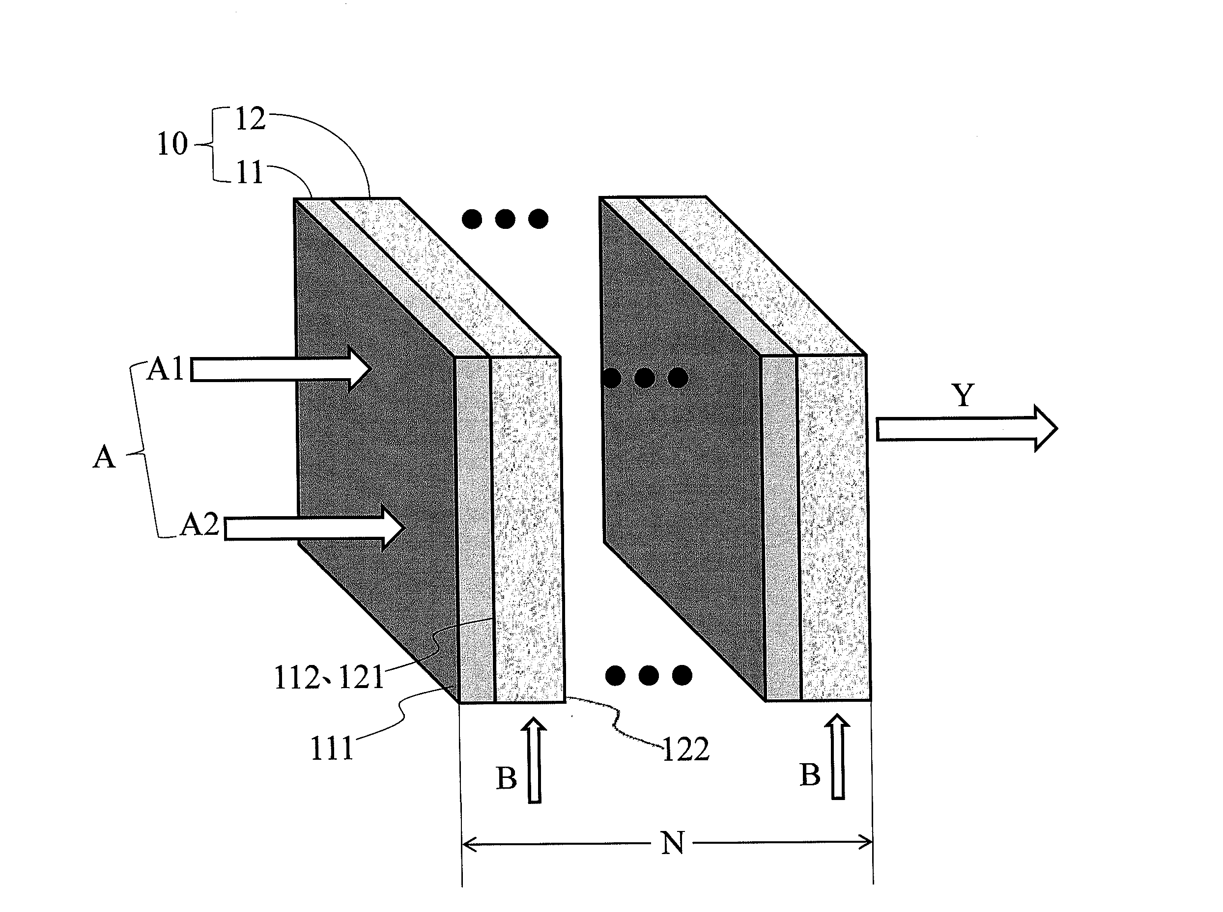
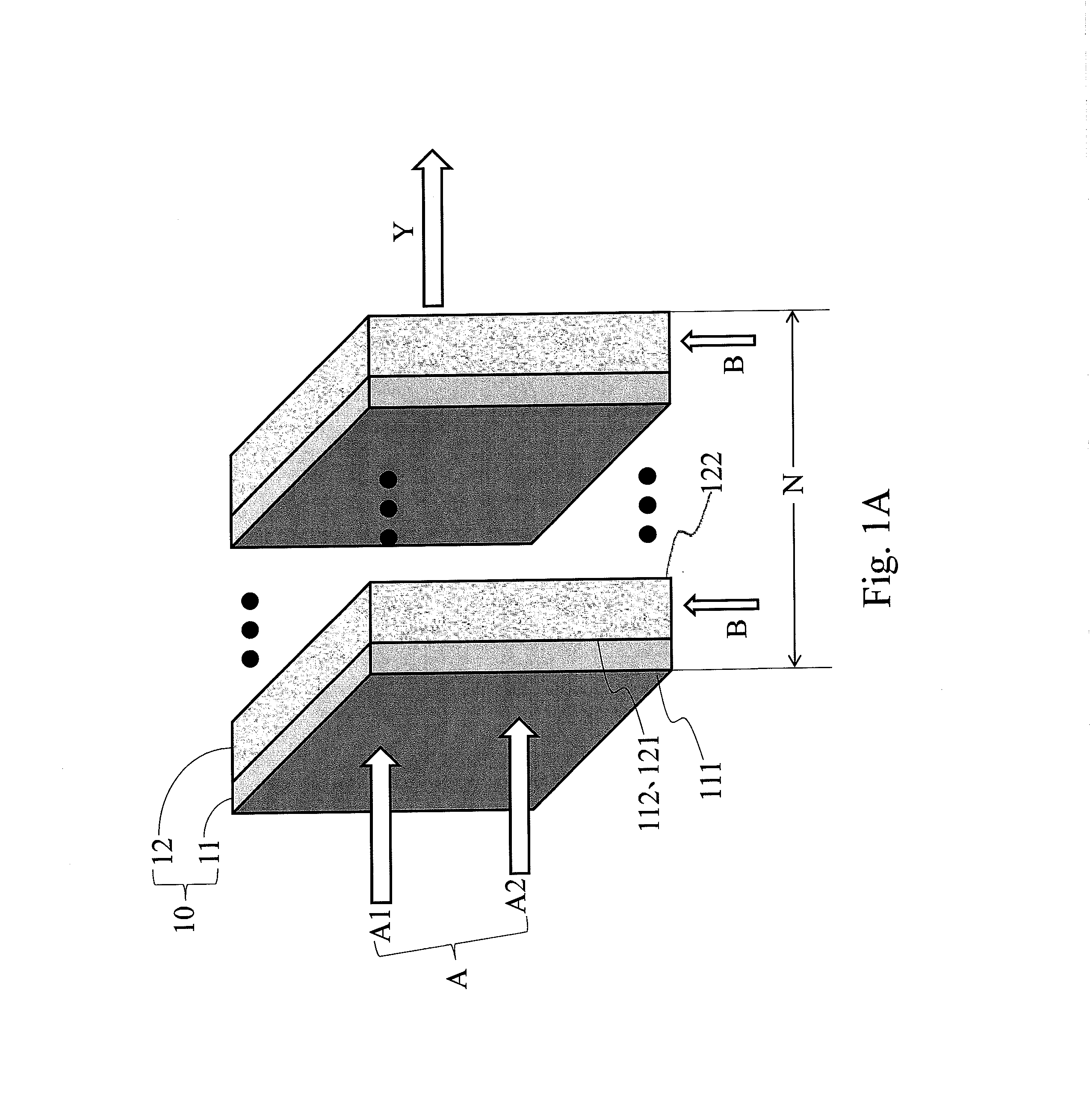
[0033]Referring to FIG. 1A, in a first preferred embodiment of the present invention, a structure with EIT-based stack layers arranged in a limited period is shown. The EIT-based photonic logic gate comprises at least N (N is greater than or equal to 1) EIT-based stack layers 10 periodically arranged. Each of the EIT-based stack layers 10 has a photonic crystal layer 11 as thick as 0.01 μm˜0.15 μm and an EIT material layer 12 as thick as 0.01 μm˜0.15 μm.

[0034]The photonic crystal layer 11 may be made of GaAs, S...


PUM


Abstract

The present invention provides an EIT-based photonic logic gate, which is constituted by EIT-based stack layers of periodic array of photonic crystal (PCs) layers and EIT (Electromagnetic Induced Transparent) material layers. The input probe signals are incident on the first photonic crystal layer, passing through one or more than one PCs-EIT interfaces and transmitted out from the last EIT material layer. Control filed as the enable signals are incident on each EIT layer to activate the optical logic gate. By varying the detune frequency of probe field and Rabi frequency of control field, its band gap structure can be adjusted. Henceforth, the tunable optical EIT-based photonic logic gate can be achieved as user required.

Description

BACKGROUND OF THE INVENTION[0001]1. Technical Field[0002]The present invention relates to photonic logic gates, and more particularly, to an EIT-based photonic logic gate that is tunable in bandwidth.[0003]2. Description of Related Art[0004]Photonic crystals are artificial periodic structures with photonic band gaps, and work by interacting with light. A photonic band gap of a periodic structure refers to a certain frequency range and any waves in the frequency range are not allowed to propagate in the periodic structure. The presence of band gaps promises photonic crystals prospects of extensive applications, because larger band gaps mean a broader band of adjustable light. When a photonic crystal is finished, its band-gap structure is fixed and its refractive index becomes unchangeable. Thus, when a different refractive index is needed, the only way is to make another photonic crystal with the desired refractive index.[0005]While photonic logic gates have been discussed in some re...

Claims


Application Information

Patent Timeline
IPC IPC(8): G02F3/00
CPCG02F2202/32G02F3/00
Inventor LIAU, TEH-CHAUSHEN, JIAN-QIWU, JIN-JEIYANG, TZONG-JER
Owner CHUNG HUA UNIVERSITY
Why Eureka
Try Eureka