Nanophotonic devices based on quantum systems embedded in frequency bandgap media

a quantum system and quantum technology, applied in the direction of active medium materials, semiconductor lasers, instruments, etc., can solve the problems of long switching time and high power requirements, response time limit the switching time of the device, and significant practical challenges, etc., to achieve easy control, enhance nonlinearity, and high efficiency

Inactive Publication Date: 2005-08-25
ALTAIR CENT
View PDF10 Cites 62 Cited by
  • Summary
  • Abstract
  • Description
  • Claims
  • Application Information

AI Technical Summary

Benefits of technology

[0015] Another object of the invention is to dramatically enhance nonlinearity in the proposed system as required for fabrication of highly efficient electro-optical and nonlinear optical materials for various electro-optical and all-optical devices.
[0016] Further object of the invention is to provide high efficiency nanoscale electro-optical modulators and converters transforming electrical signals into optical and operating as switches, modulators, transistors or control-NOT logic gates. Again, due to resonance character of coupling between passband photons and the working transition of quantum systems, the coupling is easily controlled by an electric field applied to the quantum system. Due to the Stark effect in atoms and molecules, or its analog in quantum dots, the applied electric filed shifts the transition frequency, and thus effectively changes propagation of the passband photons in quantum system waveguides.
[0017] Still another object of the invention is to provide efficient lines of delay of optical pulses with required group velocity of passband light pulses propagating along the quantum system waveguide.

Problems solved by technology

The emerging competition between all-optical devices and their electronic counterparts brings with it significant practical challenges.
The major drawbacks of such all-optical devices are related to their size (most of the devices cannot be scaled down to spatial extensions smaller than 300 μm), their long switching times and their high power requirements.
Cavity build-up time, cavity dynamical effects and nonlinear medium response time limit the switching time of the device.
Consequently the product of the switching threshold and switching time remains unacceptably large.
Using materials with relatively large optical nonlinearities also requires a compromise in the response time of the medium.
Other physical limitations include the lack of scalability and integrability.
However, due to fast spontaneous decay of the surface plasmon polaritons, loss in chain waveguides made form the metallic nanoparticles are unacceptably high for practical implementations.
Therefore, they cannot be used for engineering all-optical devices, where light signal is controlled by another light.
Even filling out of the cavities with a nonlinear optical medium could not result in strong nonlinear properties required for all-optical signal processing because of relatively weak optical nonlinearities of conventional nonlinear optical media.
Moreover, switching time of the quantum system from one discrete state to another can be obviously extremely short.
However, in vacuum or in conventional optical media, an excited state of the quantum system spontaneously decays vary fast into propagating electromagnetic modes that essentially restricts practical implementations of strong resonance nonlinearity in all-optical devices.

Method used


Image

  • Nanophotonic devices based on quantum systems embedded in frequency bandgap media
  • Nanophotonic devices based on quantum systems embedded in frequency bandgap media
  • Nanophotonic devices based on quantum systems embedded in frequency bandgap media

Examples


Embodiment Construction

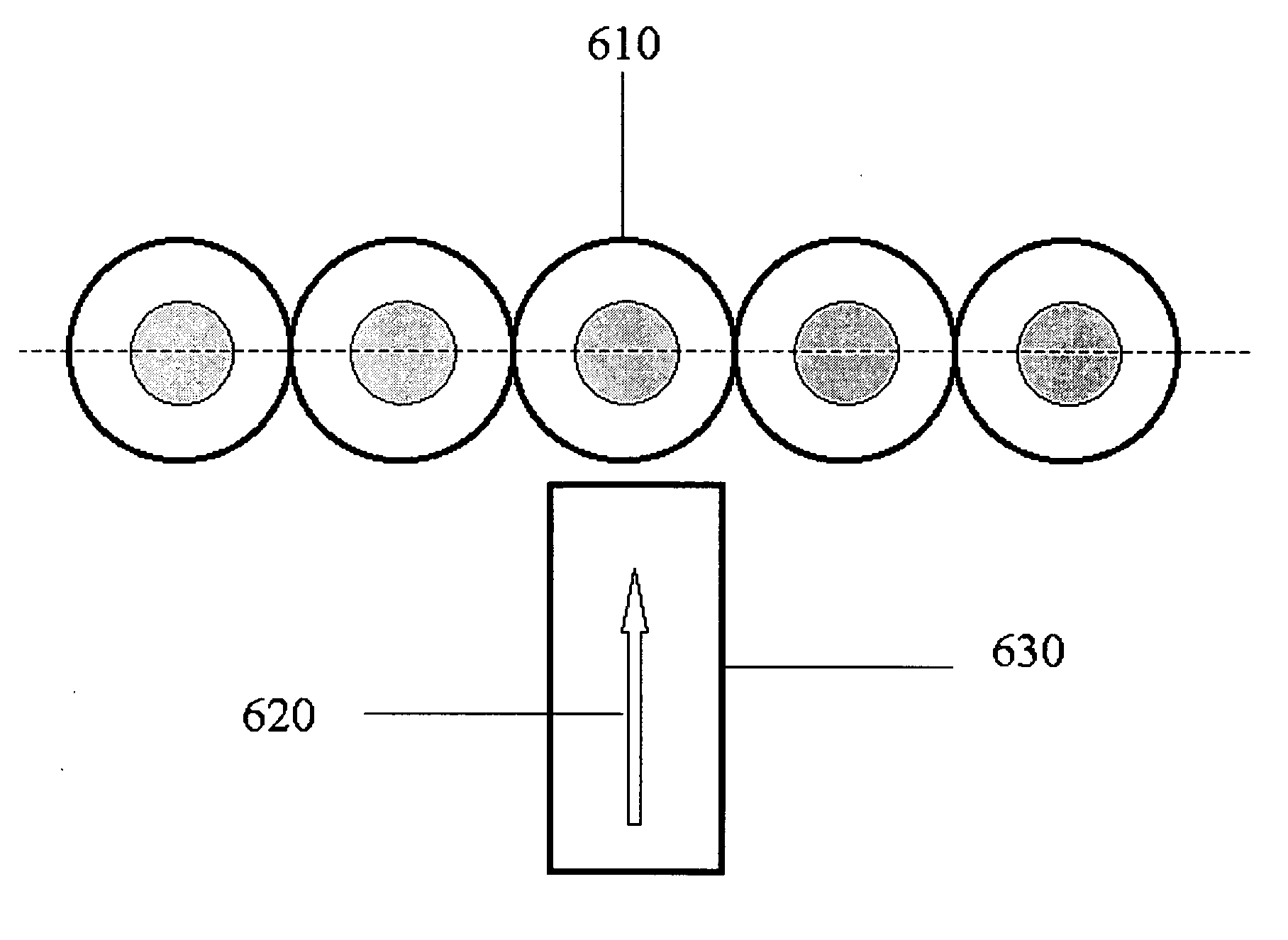
[0033] The preferred embodiments are directed to a new type of nanophotonic materials, devices and integrated nanophotonic circuits for both classical and quantum optical signal processing, including optical quantum computing, transmission and generation of light. A key element of the preferred embodiments of nanophotonic devices is a waveguide made of quantum systems embedded in a frequency bandgap medium, provided that the transition frequency of at least one of the optical transitions of the quantum systems lies inside the photonic bandgap of the frequency bandgap medium. The present invention will be more clearly understood and further applications will be apparent when detailed descriptions of preferred embodiments of the invention are made for a specific realization of the invention based on semiconductor quantum dots embedded in photonic crystals (photonic bandgap materials). Moreover, making use of the quantum dots for practical implementation of quantum system waveguides ha...


PUM


Abstract

The present invention describes nanophotonic materials and devices for both classical and quantum optical signal processing, transmission, amplification, and generation of light, which are based on a set of quantum systems having a discrete energy levels, such as atoms, molecules, or quantum dots, embedded in a frequency bandgap medium, such as artificial photonic crystals (photonic bandgap materials) or natural frequency dispersive media, such as ionic crystals, molecular crystals, or semiconductors, exhibiting a frequency (photonic) bandgap for propagating electromagnetic modes coupled to optical transitions in the quantum systems. If the frequency of one of optical transitions, called the working transition, lies inside the frequency bandgap of the medium, then spontaneous decay of the working transition into propagating photon modes is completely suppressed. Moreover, the excitation of the working transition and a photon form a photon-quantum system bound state lying inside the photonic bandgap of the medium, in which radiation is localized in the vicinity of the quantum system. In a quantum system “wire” or a quantum system “waveguide”, made of spatially disordered quantum systems, or in a chain quantum system waveguide made of a periodically ordered identical quantum systems, wave functions of the photon-quantum system bound states localized on different quantum systems overlap each other and develop a photonic passband lying inside bandgap of the photonic bandgap medium. Photons with frequencies lying inside the photonic passband propagate along the quantum system waveguide. Since the working transition cannot be excited twice, the passband photons interact with each other extremely strongly both in one waveguide and in different waveguides that are located sufficiently close to each other. These unique nonlinear properties of the quantum system waveguides are proposed to use for engineering key nanophotonic devices, such as all-optical and electro-optical switches, modulators, transistors, control-NOT logic gates, nonlinear directional couplers, electro-optical modulators and converters, generators of entangled photon states, passband optical amplifiers and lasers, as well as all-optical integrated circuits for both classical and quantum optical signal processing, including quantum computing.

Description

BACKGROUND OF THE INVENTION [0001] 1. Field of the Invention [0002] This invention relates to nanophotonic materials, devices and integrated chips for both classical and quantum optical signal processing based on nanoscale size spatially ordered or disordered structures of quantum systems, such as atoms, molecules, quantum dots, etc, embedded in frequency bandgap media, such as artificial photonic crystals (photonic bandgap materials) or natural ionic crystals, molecular crystals, and semiconductor materials exhibiting a frequency gap in their spectrum of elementary electromagnetic excitations. Preferred embodiments include all-optical nanoscale integrated circuits and such key elements of nanophotonics, as efficient lines of delay, switches, modulators, transistors, linear and nonlinear directional couplers, efficient generators of photons in entangled states, optical amplifiers, lasers, etc., utilizing linear and, especially, unique nonlinear properties of quantum systems in the f...

Claims


Application Information

Patent Timeline
Patent Type & Authority Applications(United States)
IPC IPC(8): G02B6/10G06N99/00H01S5/00H01S5/14H01S5/34
CPCB82Y10/00B82Y20/00H01S5/3412G06N99/002H01S5/14G02B6/10G06N10/00
Inventor RUPASOV, VALERYKRIVOSHLYKOV, SERGEI
Owner ALTAIR CENT
Why Eureka
Try Eureka