Metal nano-void photonic crystal for enhanced raman spectroscopy

A metal and plasma technology, applied in the field of Raman spectroscopy, can solve problems such as monolithic integration that have not been studied or identified, and achieve the effects of reducing complexity, large reproducibility, and increasing productivity

Inactive Publication Date: 2007-10-17
D3 TECH
View PDF8 Cites 59 Cited by
  • Summary
  • Abstract
  • Description
  • Claims
  • Application Information

AI Technical Summary

Problems solved by technology

However, conducting SPPs inside the pores and conducting SPPs on the metal face as well as localized SPPs confined to surface defects (and their coupling) have not been investigated in the context of Raman signal enhancement for use as biosensors. These combinations of SPP etc.
Also, no researchers in this field have identified the benefits of segmenting the light collected and extracted from the Raman signal and the possible monolithic integration of signal modulation functions before and after the Raman generation process

Method used


Image

  • Metal nano-void photonic crystal for enhanced raman spectroscopy
  • Metal nano-void photonic crystal for enhanced raman spectroscopy
  • Metal nano-void photonic crystal for enhanced raman spectroscopy

Examples


Embodiment Construction

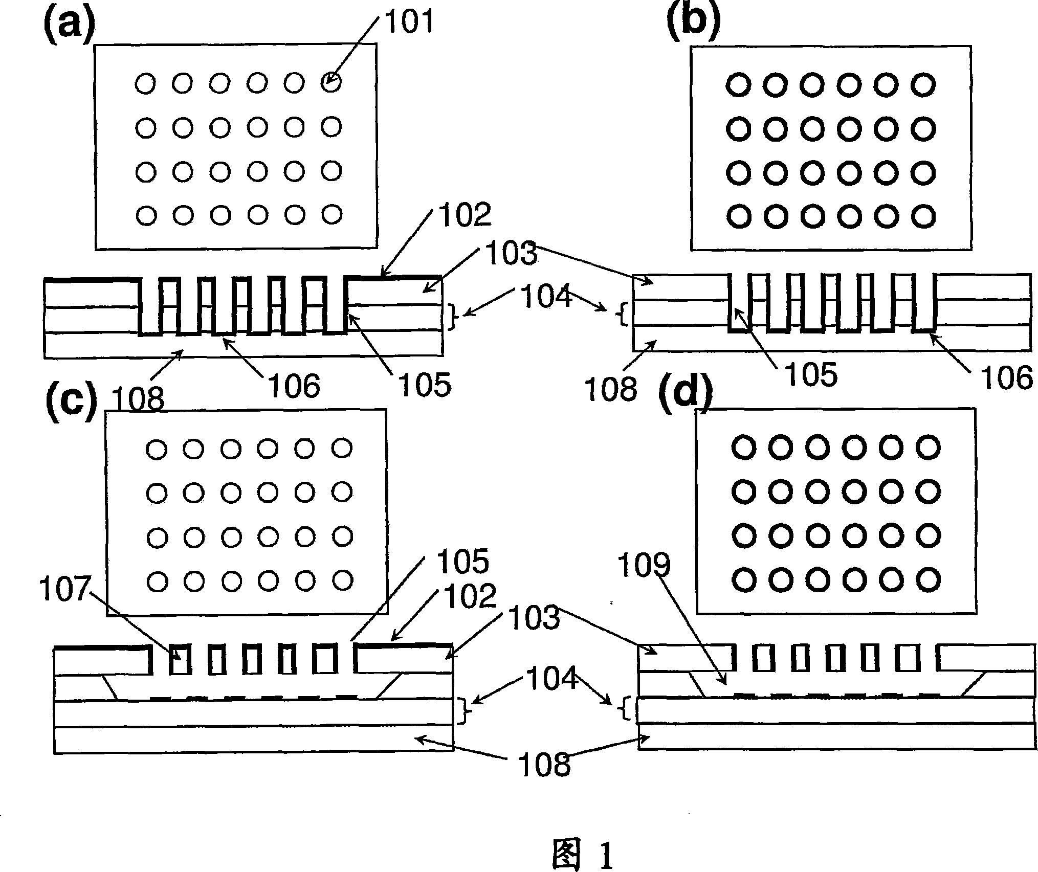
[0059] SERS active platform

[0060] The main aspect of the invention is a planar platform for receiving light radiation from a light source, as will now be described.

[0061] In a first embodiment of the platform depicted in FIG. 1( a ), the platform comprises a dielectric layer with a predefined surface modulation (patterned structure) of continuous metal dielectric coatings 102 , 105 , 106 .

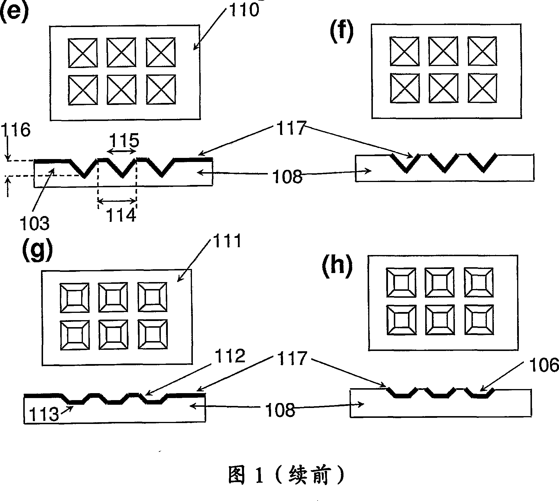
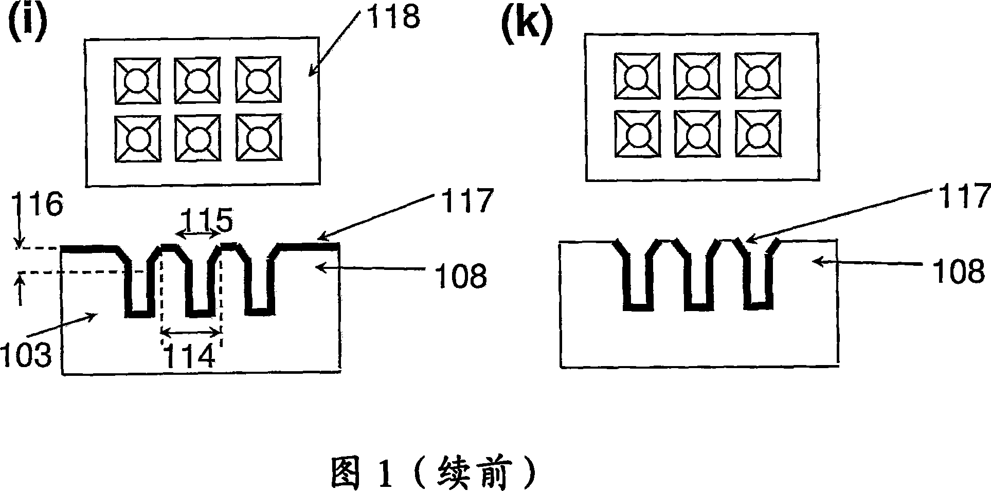
[0062] Surface modulation is achieved by the definition of a 2D periodic array of holes and recesses 101 embedded in an otherwise planar dielectric surface 103 . Distributions of 2D periodic lattice structures include, but are not limited to, square, triangular, and rectangular lattice geometries. The array of holes can also be arranged to form a graded or doubly graded 2D photonic crystal lattice, a quasi-periodic photonic crystal, or a lattice structure with one or more defects. If the array of holes is arranged in a regular lattice, it will be characterized by a typical lattice ...


PUM

PropertyMeasurementUnit
diameteraaaaaaaaaa
depthaaaaaaaaaa
thicknessaaaaaaaaaa

Abstract

A planar optical platform for generating a Raman signal from a foreign object comprises an input region and an output region, for receiving and extracting optical radiation, optically coupled to a plasmonic band structure region. The plasmonic band structure region comprises a layer of a first material, having a first refractive index, patterned with an array of sub-regions of a second material, having a second refractive index, wherein a side-wall of each sub-region is coated with a metallodielectric layer. The array of sub-regions gives rise to a plasmonic band structure and, in use, each sub-region confines a plasmon resonance excited by optical radiation coupled into the plasmonic band structure region, which gives rise to a Raman signal from a foreign object placed proximate the plasmonic band structure region. The platform may be incorporated into a spectroscopic measurement system and is particularly useful for surface-enhanced Raman spectroscopy of analyte molecules.

Description

technical field [0001] The invention relates to Raman spectroscopy, in particular to an optical platform for surface-enhanced Raman spectroscopy. Background technique [0002] Raman spectroscopy can be used for a variety of purposes, although it can also be used to study other quantized entities, it is usually mainly used to study vibrational quantum numbers, for example, the vibrations of molecules or photons in solids. Raman spectroscopy can provide detailed information about the physical state of a sample material and can be used to distinguish states of different but chemically consistent molecules (eg, various molecular isomers) from one another. [0003] Raman spectroscopy has a wide range of applications in many different industries, for example, Raman spectroscopy is used in pharmaceuticals, chemicals, bioanalysis, medical care, materials science, art restoration, polymers, semiconductors, gemology, forensics, survey research, There are applications in the fields of...

Claims


Application Information

Patent Timeline
Patent Type & Authority Applications(China)
IPC IPC(8): G01N21/55G01N21/65
CPCG01N21/658B82Y30/00B82Y15/00G01J3/44G01N21/65
Inventor 杰里米·邦伯格斯文·曼科普夫马吉德·祖罗布约翰·林肯詹姆斯·威尔金森
Owner D3 TECH
Why Eureka
Try Eureka