Waveguiding structures with embedded microchannels and method for fabrication thereof

a waveguide and microchannel technology, applied in the field of waveguide structures with embedded microchannels and methods for fabrication thereof, can solve the problems of reducing the fabrication process, prohibitively expensive fabrication, and unable to disclose planar waveguide structures with photonic band gaps

Inactive Publication Date: 2005-12-29
HER MAJESTY THE QUEEN & RIGHT OF CANADA REPRESENTED BY THE MIN OF IND THROUGH THE COMM RES CENT
View PDF5 Cites 65 Cited by
  • Summary
  • Abstract
  • Description
  • Claims
  • Application Information

AI Technical Summary

Problems solved by technology

While for obtaining a true photonic crystal, wherein light propagation is prohibited in all three dimensions for certain wavelengths, fabrication of true 3D arrays of micro-voids is generally required, such fabrication can be prohibitively expensive.
However, to the best of the inventor's knowledge, no planar waveguiding structures with photonic band gaps have been disclosed wherein the microchannels are oriented in-plane with the substrate, along the waveguiding direction.
However, these prior-art method for formation of enclosed microchannels crossing waveguides have several drawbacks.
The additional step of bonding or gluing a top cover plate technique is outside of common commercial techniques of silicon processing, and complicates the fabrication process.
Microchannel structures fabricated using this process are limited to a single layer.
The microchannels are typically located at the surface, are difficult to seal and fragile.
The use of single-point liquid-optical field interaction, wherein the fluid interacts with an optical mode only in points of microchannel-waveguide interactions, greatly limits the interaction length and thus reduces beneficial effects of such interactions.
Also, the cover-plate techniques typically provide microchannels which have substantially trapezoidal or rectangular cross-sections with shapes which are difficult to control.

Method used


Image

  • Waveguiding structures with embedded microchannels and method for fabrication thereof
  • Waveguiding structures with embedded microchannels and method for fabrication thereof
  • Waveguiding structures with embedded microchannels and method for fabrication thereof

Examples


Embodiment Construction

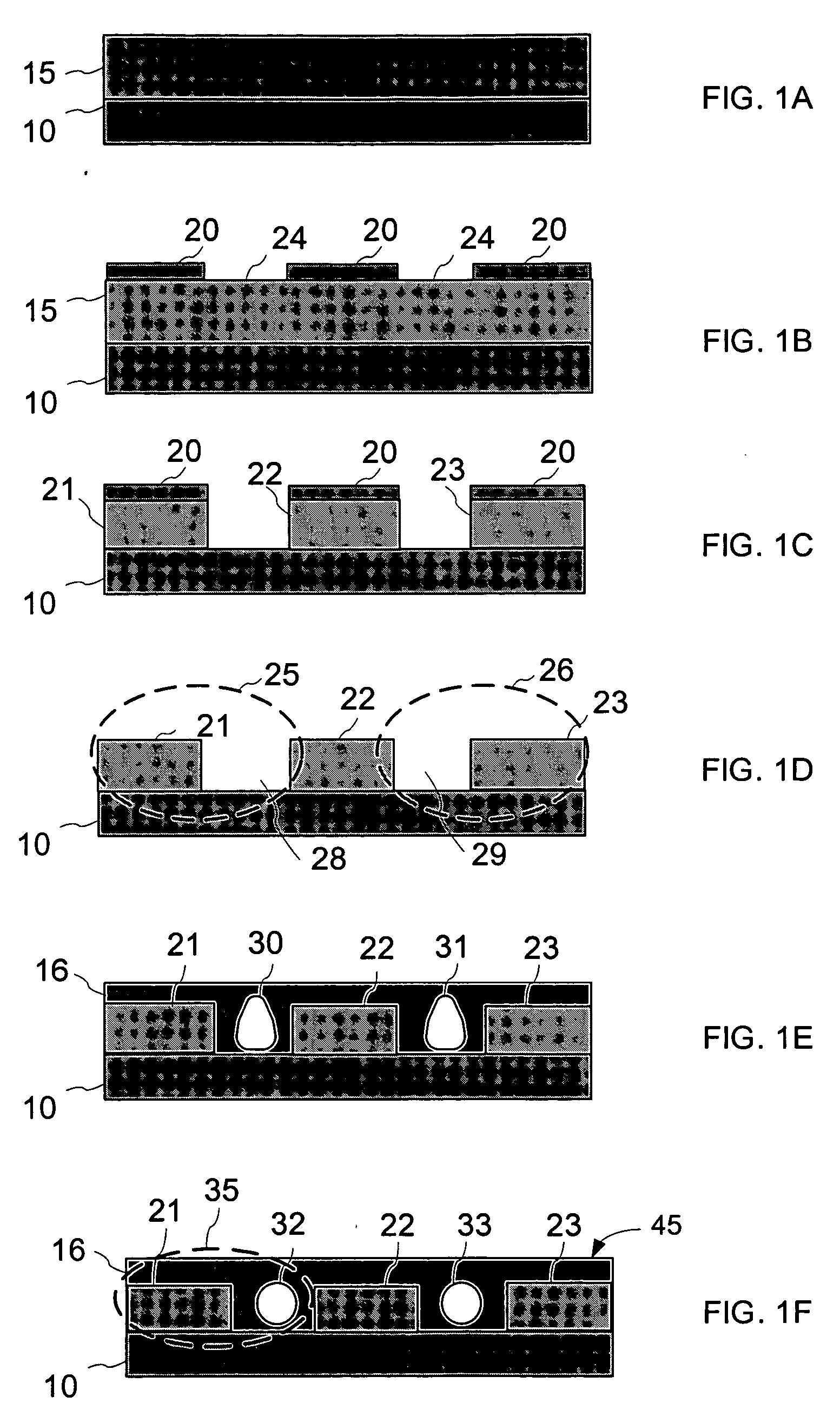
[0042] First, the method of the present invention for fabricating waveguiding structures with microchannels embedded therein will now be described with reference to FIGS. 1A-1F, illustrating main steps of the method in one exemplary embodiment thereof.

[0043] In this embodiment, the method starts with depositing a layer 15 of a first optical material on a planar substrate 10, resulting in a planar structure shown in FIG. 1A. The planar substrate 10 is preferably a silicon substrate, but can be also any other substrate, for example made of any other semiconductor or dielectric material, such as glass, or a ceramic, on which the optical material 15 can be deposited to form a monolithic structure.

[0044] In the context of this specification, the term “planar”, used in relation to a substrate, means that a relevant portion of said substrate has a main surface and a radius of curvature thereof substantially exceeding dimensions of geometrical features of the present invention formed over...


PUM

PropertyMeasurementUnit
depthaaaaaaaaaa
depthaaaaaaaaaa
depthaaaaaaaaaa

Abstract

The invention provides a method for fabricating planar waveguiding structures with embedded microchannels. The method includes the step of depositing, over a planar template having at least one indented feature comprising a ridge of a first optical material and a narrow trench adjacent thereto, a second optical material, and the step of subsequent annealing thereof, so that an embedded hollow microchannel forms within the trench. The method provides planar structures wherein the ridge and the embedded microchannel cooperate to form an optical waveguiding structure having a waveguiding direction collinear with the embedded microchannel. Embodiments of the method for forming microfluidic devices integrating ridge waveguides with hollow microchannels having surface access points for fluid delivery, and for forming photonic crystals, are disclosed together with corresponding device embodiments.

Description

CROSS-REFERENCE TO RELATED APPLICATIONS [0001] The present invention claims priority from U.S. Provisional Patent Application No. 60 / 583,365 filed Jun. 29th, 2004, entitled “Novel Method for Fabricating Uniform, Micron-Sized, Embedded Arrays of Channels in Silica Glass Layer Structures”, which is incorporated herein by reference.TECHNICAL FIELD [0002] The present invention relates to methods of fabricating planar waveguiding structures with integrated embedded microchannels and microchannel arrays, and to optical devices incorporating microfluidic channels coupled to optical waveguides. BACKGROUND OF THE INVENTION [0003] Optical waveguiding structures incorporating embedded hollow microchannels and microchannel arrays are used in a variety of applications, ranging from waveguides in three-dimensional (3D) and two-dimensional (2D) photonic bandgap materials, or photonic crystals, to microfluidic systems for optical detecting and testing microscopic quantities of organic and non-organ...

Claims


Application Information

Patent Timeline
Patent Type & Authority Applications(United States)
IPC IPC(8): G01N21/03G02B6/10G02B6/12G02B6/122G02B6/13G02B6/132H01J40/14H01L21/00
CPCB82Y10/00B82Y20/00G01N21/0303G02B6/10G02B2006/12176G02B6/1225G02B6/13G02B2006/12169G02B2006/12173G02B6/122
Inventor DUMAIS, PATRICKLEDDERHOF, CHRISCALLENDER, CLAIREBLANCHETIERE, CHANTALNOAD, JULIANLOVELL, GLENDON
Owner HER MAJESTY THE QUEEN & RIGHT OF CANADA REPRESENTED BY THE MIN OF IND THROUGH THE COMM RES CENT
Why Eureka
Try Eureka