Optoelectronic substrate

a technology of optoelectronic substrates and substrates, applied in the direction of optical elements, circuit optical details, instruments, etc., can solve the problems of increasing processing speed, electromagnetic radiation interference noise (emi), and affecting so as to reduce electromagnetic interference caused by electromagnetic emission noise, the heat release ability of optoelectronic wiring substrates can be improved, and the heat release ability of optoelectronic wiring substrates

Inactive Publication Date: 2005-08-30
CANON KK
View PDF26 Cites 65 Cited by
  • Summary
  • Abstract
  • Description
  • Claims
  • Application Information

AI Technical Summary

Benefits of technology

[0022]The waveguide characteristics and the optical coupling characteristics can be controlled by designing suitably the repeating period and the like of the photonic crystal, and thereby the freedom degree in designing the optical circuit like routing can be increased.
[0024]In this second embodiment, the anodized alumina insulates electrically the electric devices and the optical devices mounted thereon, and serves as an optical wiring and an optical coupler, whereby the optoelectronic wiring device can be made compact by a simple technique, and further the electromagnetic emission noise can be reduced, enabling high-speed data processing with high reliability.
[0026]Further, the heat releasing ability of the optoelectronic wiring substrate can be improved by placing the anodized alumina on a metal base plate such as an aluminum plate. Filling of the anodized alumina holes with an electroconductive material makes the anodized alumina useful as an electric wiring for connecting electrically the electronic devices or the optical devices.
[0027]Filling of the anodized alumina holes with a magnetic material makes the anodized alumina useful as an electromagnetic wave absorber, which gives an optoelectronic wiring substrate less sensitive to electromagnetic emission noise. Thus by placing suitably the filled anodized alumina, electromagnetic interference caused by the electromagnetic emission noise can be reduced.
[0028]Furthermore, the anodized alumina can be produced in a large area readily at a low cost, advantageously.

Problems solved by technology

However, with increase of the processing speed, the adverse effect of wiring delay has become remarkable.
However, the increase of the processing speed has given rise to another problem of electromagnetic radiation interference noise (EMI).
Consequently, when signals flow in a high speed through adjacent wirings, the electromagnetic waves can interfere with each other to cause noises, preventing precise transmission of the signals.
In particular, in mobile terminals, which are coming to be driven at a lower voltage and higher electric current intensity, the adverse effect of the EMI is becoming serious.
However, this is not satisfactory in the production cost and yield.

Method used


Image

  • Optoelectronic substrate
  • Optoelectronic substrate
  • Optoelectronic substrate

Examples


first embodiment

(First Embodiment)

[0044]An embodiment of the optoelectronic substrate of the present invention is explained below. In the description below, the optoelectronic substrate is occasionally referred to as an “optoelectronic wiring substrate”, but the both terms indicate the same thing.

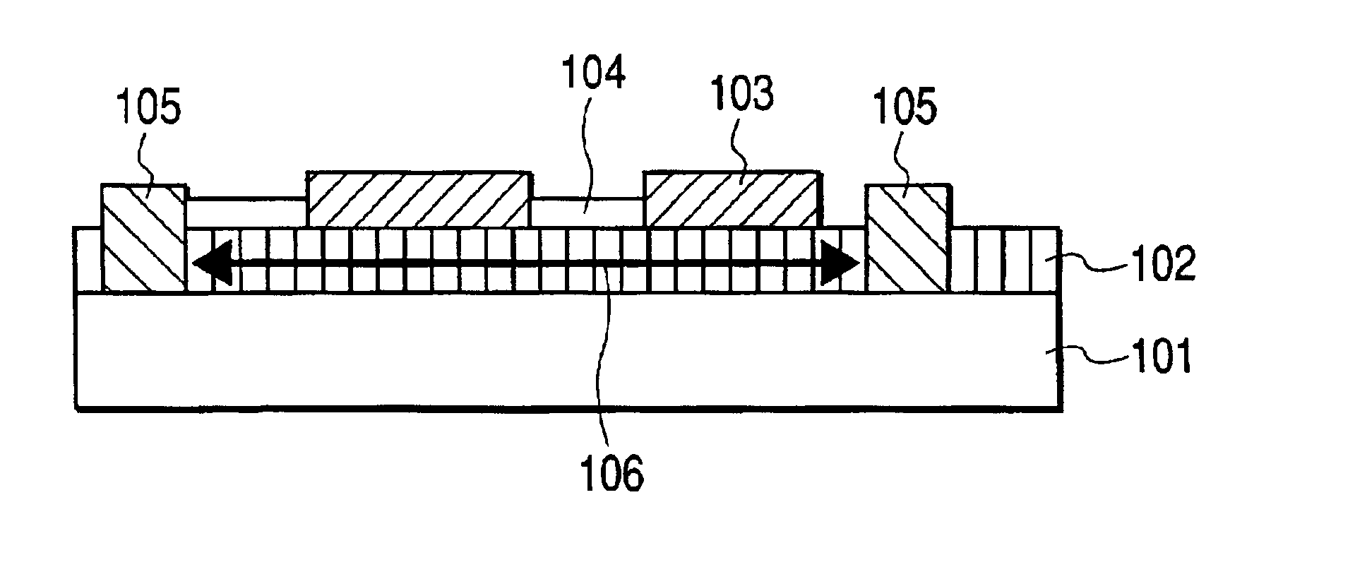
[0045]FIG. 12 is a schematic sectional view for explaining an example of an optoelectronic wiring substrate of the present invention. In FIG. 12, the numeral 101 indicates a base plate; 109, a periodic structure such as a photonic crystal; 103, an electronic device formed on the surface of the photonic crystal; 104, an electric wire serving as an optical wiring layer formed on the photonic crystal: and 105, an optical device. The arrow 106 shows schematically the transmission of light through the photonic crystal.

[0046]In FIG. 12, although plural electronic devices and plural optical devices are formed on base plate 101: the respective devices need not necessarily be provided in plurality.

(Photonic Crystal...

second embodiment

(Second Embodiment)

[0089]A second embodiment of the present invention is described below in which anodized alumina is employed as the optical waveguide constituting an optical wiring layer.

[0090]The anodized alumina is sufficiently effective as the optical waveguide. Further, the anodized alumina of a photonic crystal structure having a regular hole arrangement will function in the same manner as shown in First Embodiment above.

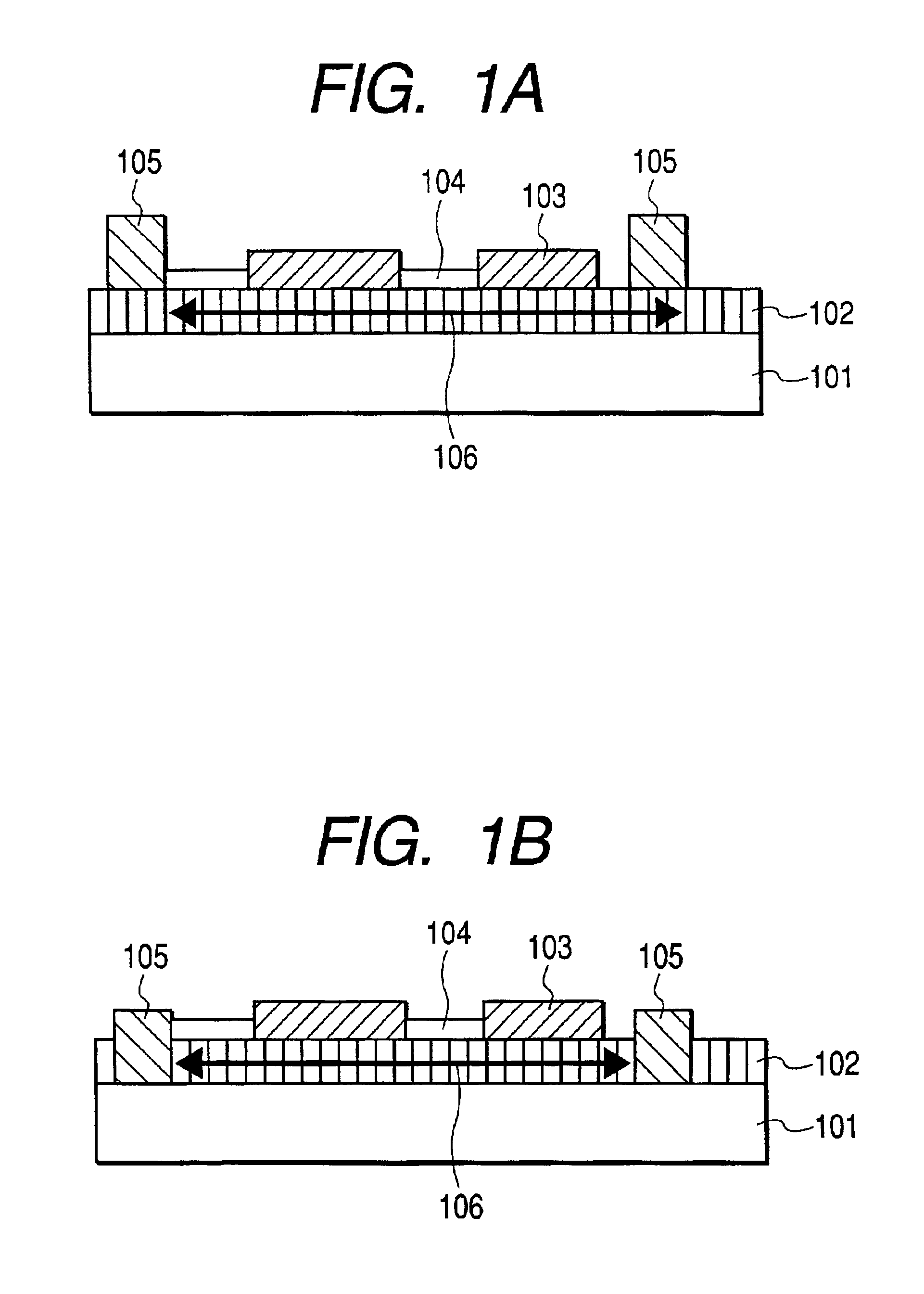
[0091]In this embodiment, an electronic device, an optical device, and electric wiring are provided on a substrate having an anodized alumina layer formed thereon as shown in FIG. 1A. The anodized alumina has a function of an insulating layer and a function of an optical waveguide to couple optically the optical devices. The anodized alumina works as the optical wiring layer.

[0092]The anodized alumina which has an insulating property insulates electrically the devices. An electric circuit can be formed by forming electric wiring thereon. Further thereon, an o...

example 1

[0137]In this Example, anodized alumina was formed on an aluminum plate, and thereon an electric device and an optical device were mounted as illustrated in FIGS. 1A and 1B.

[0138]Firstly, on an aluminum plate, anodized alumina 102 was formed in a thickness of 5 μm. The remaining unanodized portion serves as base plate 101.

[0139]Prior to the anodization, hole-starting points (concaves) were formed on the surface of the aluminum plate by FIB irradiation. This enables the holes regularly arranged in a honeycomb state (triangular lattice state). In this example, a focused ion beam of Ga was projected to form hole-starting points in dots arranged in 360 nm intervals in triangular lattice arrangement, with ion species of Ga, at acceleration voltage of 30 kV, ion beam diameter of 100 nm, ion current of 300 pA, and irradiation time for each dot of 10 msec.

[0140]The anodization was conducted with an apparatus illustrated in FIG. 11, in a 0.3M phosphoric acid bath as the anodization electroly...


PUM


Abstract

An optoelectronic substrate comprises an electronic device, an optical device, and an optical wiring layer, the optical wiring layer comprising a photonic crystal. An optoelectronic substrate comprises an electronic device, an optical device, and an optical wiring layer, wherein the optical wiring layer is comprised of a periodic structure having a repeating period nearly equal to or smaller than the wavelength of light employed for signal transmission. An optoelectronic substrate comprises an electronic device, an optical device, an electric wiring connected to the electronic device, an optical wiring layer, and a base plate, wherein the optical wiring layer is employed as an insulating layer between the base plate and the electric wiring.

Description

BACKGROUND OF THE INVENTION[0001]1. Field of the Invention[0002]The present invention relates to an optoelectronic substrate, particularly to a circuit substrate having an electronic device and an optical device in combination.[0003]2. Related Background Art[0004]In recent years, data processing apparatuses such as portable telephones and personal digital assistance (PDA) are required to have a high-speed processing ability, a small size, and a light weight simultaneously. However, with increase of the processing speed, the adverse effect of wiring delay has become remarkable. To prevent the wiring delay, the simplest way is to shorten the wirings inside and between the chips. The wire-shortening is also helpful in miniaturizing the substrate, so that many inventions have been disclosed thereon.[0005]However, the increase of the processing speed has given rise to another problem of electromagnetic radiation interference noise (EMI).[0006]The problem of EMI is explained below.[0007]S...

Claims


Application Information

Patent Timeline
Patent Type & Authority Patents(United States)
IPC IPC(8): G02B6/13G02B6/34G02B6/122G02B6/42G02B6/43H05K1/02H05K1/05
CPCB82Y20/00G02B6/1225G02B6/13G02B6/34G02B6/42G02B6/4277G02B6/43H05K1/0274H05K1/053
Inventor IWASAKI, TATSUYADEN, TOHRU
Owner CANON KK
Why Eureka
Try Eureka