Light emitting diode structure having photonic crystals

a light-emitting diode and crystal structure technology, applied in the direction of semiconductor devices, basic electric elements, electrical apparatus, etc., can solve the problems of reducing the substrate does not effectively increase the external the external quantum efficiency cannot be increased. , to achieve the effect of increasing the internal quantum efficiency of the led structure, improving the epitaxial quality of the first type of doping semiconductor layer, and increasing the photo energy

Active Publication Date: 2007-02-06
FORMOSA EPITAXY INCORPORATION +1
View PDF4 Cites 64 Cited by
  • Summary
  • Abstract
  • Description
  • Claims
  • Application Information

AI Technical Summary

Benefits of technology

[0010]The invention provides an LED structure, having a substrate of photonic crystal. The substrate with photonic crystal can have improved the epitaxial quality. The light propagating along the substrate surface can be reduced, and thereby the light emitting efficiency of the LED structure can be increased.
[0022]In the invention, the photonic crystals are formed on the substrate surface of the LED structure, so as to improve the epitaxial quality of the first type doping semiconductor layer and thereby increase the internal quantum efficiency of the LED structure. In addition, the photonic crystals of the invention can further increase the photo energy emitted at the forward direction of the LED structure, so as to increase the external quantum efficiency of the LED structure. As a result, the LED structure of the invention has sufficiently improved light emitting efficiency.

Problems solved by technology

However, the way to randomly roughen the surface of the substrate does not effectively increase the external quantum efficiency of the LED structure.
As a result, the internal quantum efficiency of the LED structure is reduced, and therefore the external quantum efficiency cannot be increased.
It then causes the decay of light, emitted from the LED structure, and the external quantum efficiency cannot be sufficiently obtained.

Method used


Image

  • Light emitting diode structure having photonic crystals
  • Light emitting diode structure having photonic crystals
  • Light emitting diode structure having photonic crystals

Examples


Embodiment Construction

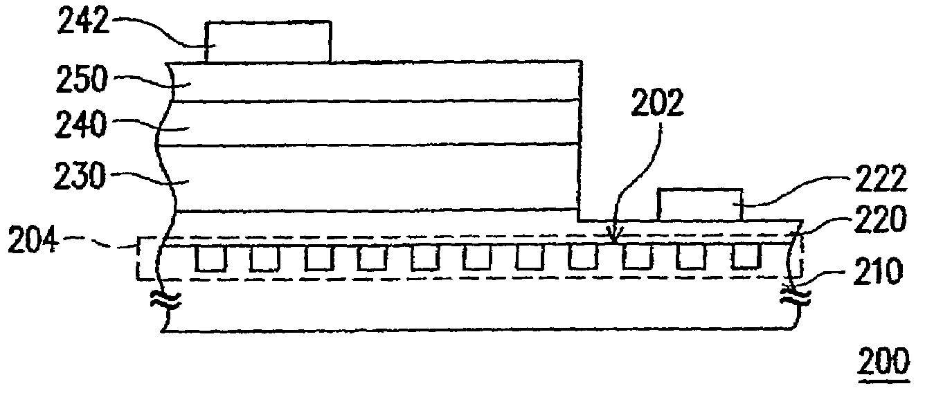
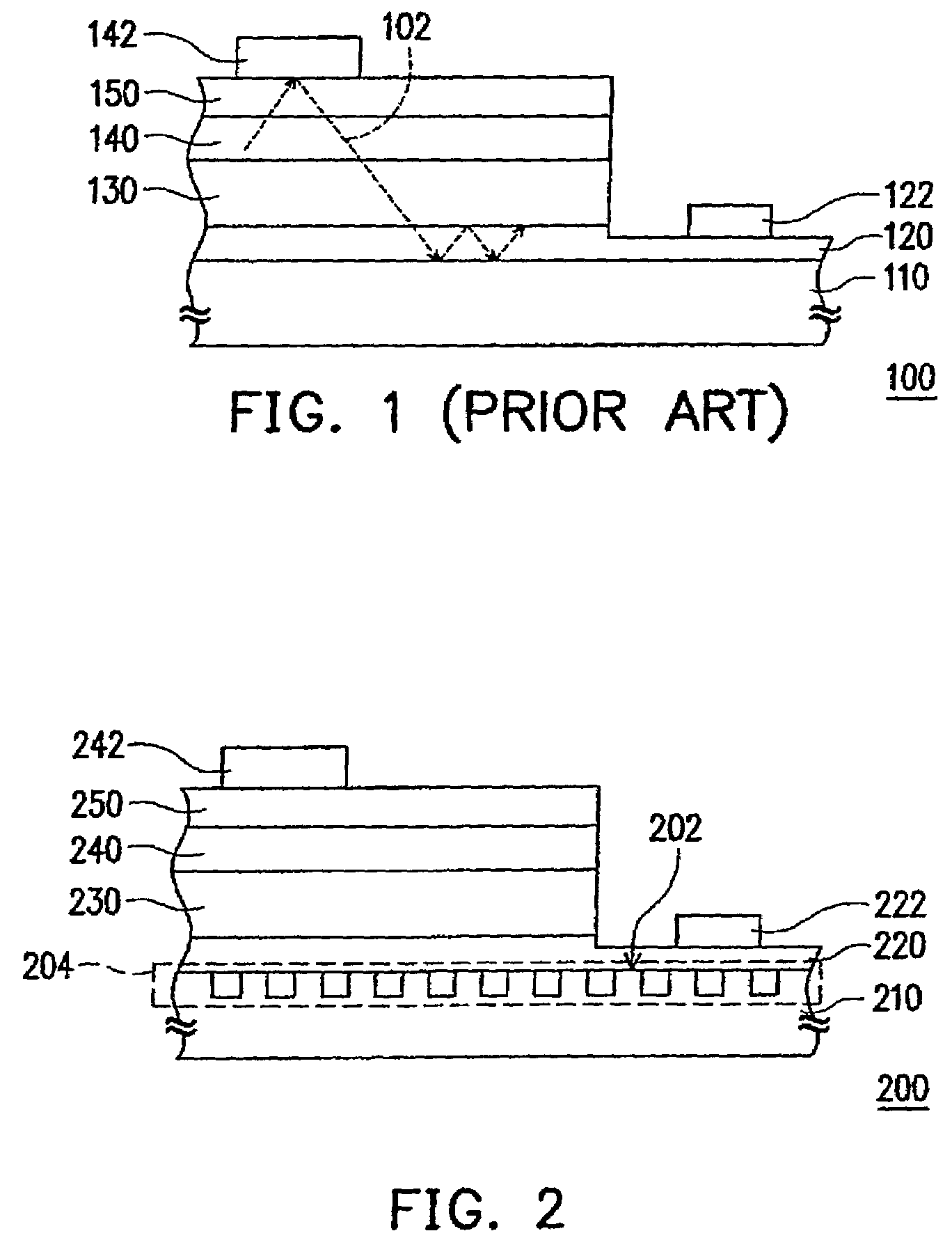
[0027]FIG. 2 is a cross-sectional view, schematically illustrating an LED structure, according to an embodiment of the invention. In FIG. 2, the LED structure 200 includes a substrate 210, a first type doping semiconductor layer 220, an electrode 222, a light emitting layer 230, a second type doping semiconductor layer 240 and an electrode 242. A material for the substrate 210 includes, for example, sapphire, silicon carborundum, spinel, or silicon substrate. The substrate 210 has a surface 202 and cylindrical photonic crystals 204 on the substrate 202.

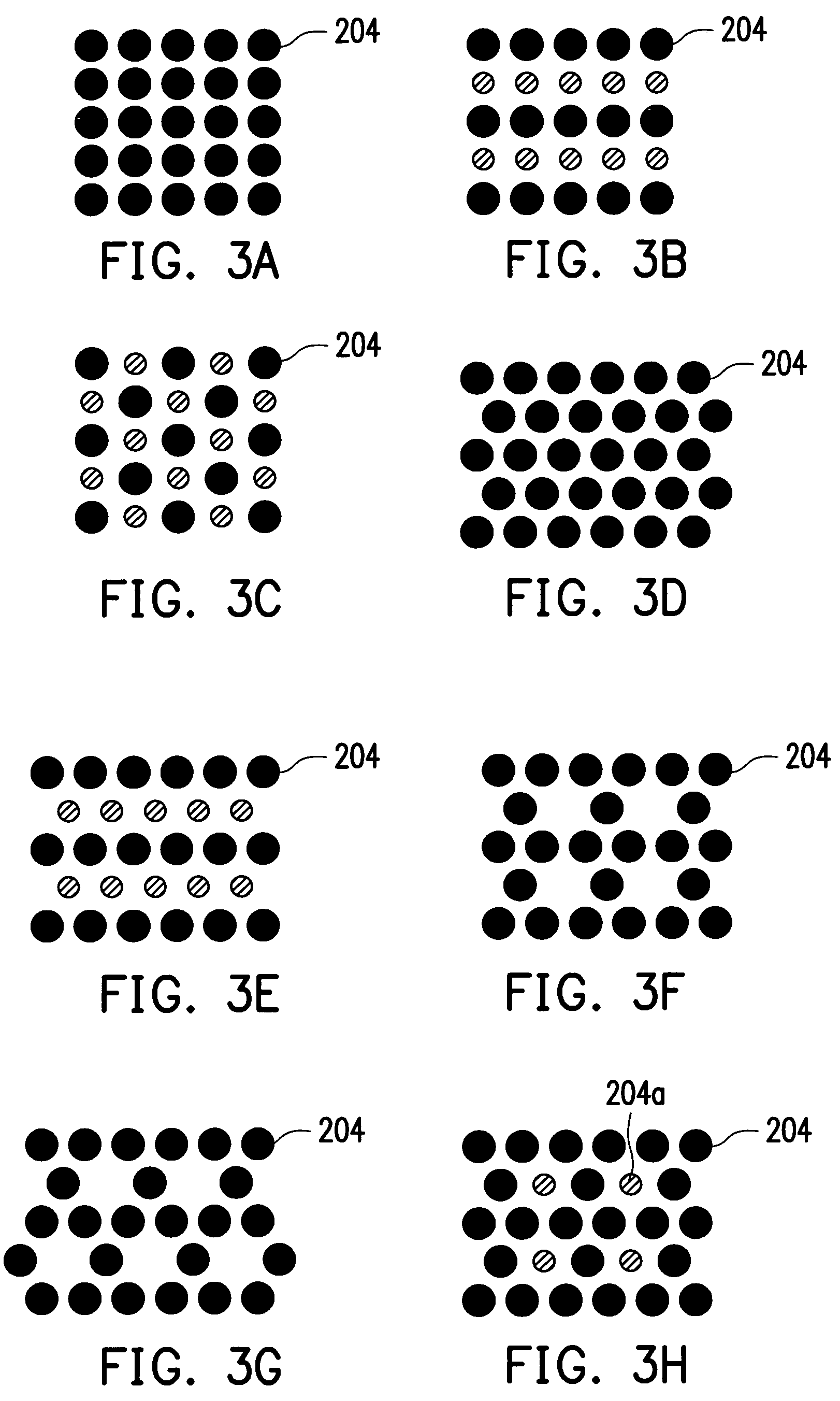
[0028]In the foregoing descriptions, the photonic crystals 204 are for example a protruding pattern or a recess pattern. The photonic crystals 204 are formed by, for example, performing photolithographic and etching processes, so as to form the cylindrical protruding pattern or cylindrical recess pattern on the surface 202. Particularly, the photonic crystals 204 are periodically arranged on the surface 202 of the substrate 210. The i...


PUM


Abstract

A light emitting diode (LED) structure includes a substrate with a surface and cylindrical photonic crystals, a first type doping semiconductor layer, a first electrode, a light emitting layer, a second type doping semiconductor layer and a second electrode. The first type doping semiconductor layer is formed on the substrate to cover the photonic crystals. The light emitting layer, the second type doping semiconductor layer and the second electrode are sequentially formed on a portion of the first type doping semiconductor layer. The first electrode is formed on the other portion of the first type doping semiconductor layer without being covered by the light emitting layer. Because the substrate with photonic crystals can improve the epitaxial quality of the first type doping semiconductor layer and increase the energy of the light forwardly emitting out of the LED, the light emitting efficiency of the LED is effectively enhanced.

Description

BACKGROUND OF THE INVENTION[0001]1. Field of Invention[0002]The present invention relates to a light emitting device. More particularly, the present invention relates to a structure of a light emitting diode.[0003]2. Description of Related Art[0004]The light emitting diode (LED), in comparing with the conventional light bulb, has significantly advantages, such as small volume, long lifetime, low voltage / current driving, non-brittle property, having no thermal issue when emitting light, containing no Hg in considering issue of environmental contamination, light emitting efficiency in saving power, and so on. In addition, the light emitting efficiency of the LED is continuously increasing in recent years, and therefore the LED has gradually taken the place of light bulb or fluorescent lamp in some application field, such as the scanner lamp with high responding speed, the back light used in liquid crystal display, the control panel light in a car, the traffic light, or the usual illum...

Claims


Application Information

Patent Timeline
Patent Type & Authority Patents(United States)
IPC IPC(8): H01L33/00H01L33/20
CPCH01L33/20H01L2933/0083
Inventor WU, LIANG-WENTSAI, YA-PINGCHIEN, FEN-RENCHANG, FU-YUYU, CHENG-TSANGWEN, TZU-CHI
Owner FORMOSA EPITAXY INCORPORATION
Why Eureka
Try Eureka