Manufacturing method of embedded epitaxial layer

A manufacturing method and epitaxial layer technology, applied in semiconductor/solid-state device manufacturing, electrical components, circuits, etc., can solve the problem of increasing particle defect size, and achieve the effect of low cost and simple process

Pending Publication Date: 2020-08-28
SHANGHAI HUALI INTEGRATED CIRCUTE MFG CO LTD
View PDF0 Cites 1 Cited by
  • Summary
  • Abstract
  • Description
  • Claims
  • Application Information

AI Technical Summary

Problems solved by technology

It can be seen that, in the step of forming the SiGe capping laye

Method used


Image

  • Manufacturing method of embedded epitaxial layer
  • Manufacturing method of embedded epitaxial layer
  • Manufacturing method of embedded epitaxial layer

Examples


Example Embodiment

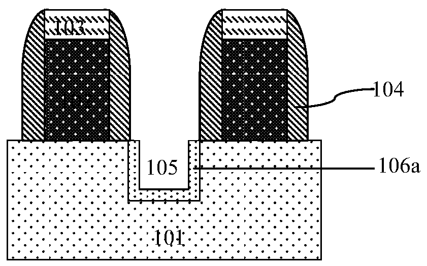
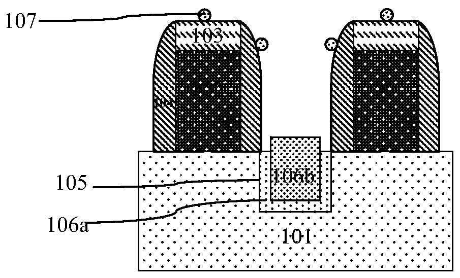
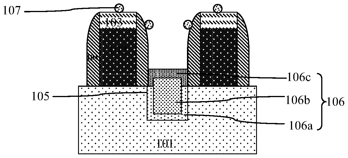
[0066] Such as figure 2 Shown is the flow chart of the exceptional extension process method of the present invention; Figure 3A to Figure 3D What is shown is a schematic diagram of the device structure in each step of the manufacturing method of the embedded epitaxial layer 6 of the embodiment of the present invention; the manufacturing method of the embedded epitaxial layer 6 of the embodiment of the present invention includes the following steps:

[0067] Step one, such as Figure 3A As shown, a dry etching process is used to form a groove 5 in the silicon substrate, and the cross section of the groove 5 has a U-shaped structure.

[0068] In the embodiment of the present invention, a gate structure is formed on the silicon substrate, and the groove 5 is self-aligned and formed in the groove 5 on both sides of the gate structure;

[0069] The gate structure includes a gate dielectric layer and a polysilicon gate 2 stacked in sequence;

[0070] A top hard mask layer 3 is covered on t...


PUM


Abstract

The invention discloses a manufacturing method of an embedded epitaxial layer. The method comprises the steps of 1, forming a U-shaped groove in a silicon substrate by adopting a dry etching process;and 2, filling an embedded epitaxial layer in the groove, wherein the step 2 comprises the sub-steps of 21, carrying out epitaxial growth to form a buffer layer; 22, carrying out epitaxial growth to form a main body layer, and forming particle defects in the growth process of the main body layer; 23, introducing an etching gas into the same epitaxial growth cavity to perform back etching so as toremove particle defects; and 24, carrying out epitaxial growth to form a cap layer. According to the invention, the particle defects generated in the epitaxial growth process of the embedded epitaxiallayer can be eliminated, so that the yield of products can be improved.

Description

technical field [0001] The invention relates to a method for manufacturing a semiconductor integrated circuit, in particular to a method for manufacturing an embedded epitaxial layer. Background technique [0002] With the development of technology, the critical dimension (CD) of the device is getting smaller and smaller. When the process node of the device is below 28nm, it is often necessary to use embedded epitaxial layers in the source and drain regions to change the stress of the channel region, thereby increasing the current carrying capacity. Mobility of electrons and thus improve the performance of the device. For PMOS devices, the embedded epitaxial layer usually adopts silicon germanium epitaxial layer (SiGe); for NMOS devices, the embedded epitaxial layer usually adopts phosphorus silicon epitaxial layer (SiP). [0003] Usually, after the gate structure of the device is formed, grooves are formed by self-alignment on both sides of the gate structure; then, an emb...

Claims


Application Information

Patent Timeline
IPC IPC(8): H01L21/8238H01L29/78
CPCH01L21/823814H01L21/823821H01L29/7848H01L29/785
Inventor 涂火金刘厥扬胡展源
Owner SHANGHAI HUALI INTEGRATED CIRCUTE MFG CO LTD
Why Eureka
Try Eureka