Light-emitting diode (LED) structure

A technology of light-emitting diodes and light-emitting layers, which is applied in the direction of electrical components, circuits, semiconductor devices, etc., can solve the problems of attenuation of light emitted from the structure of light-emitting diodes, the inability to improve external quantum efficiency, and the reduction of crystallinity of n-type doped semiconductor layers. Effect of increasing internal quantum efficiency, improving external quantum efficiency, and good luminous efficiency

Inactive Publication Date: 2010-10-13
江苏璨扬光电有限公司
View PDF2 Cites 2 Cited by
  • Summary
  • Abstract
  • Description
  • Claims
  • Application Information

AI Technical Summary

Problems solved by technology

[0007] However, arbitrarily roughening the substrate surface cannot effectively improve the external quantum efficiency of the LED structure.
On the one hand, when the concave pattern or the convex pattern on the surface of the substrate is too large, the crystallinity of the n-type doped semiconductor layer grown on the surface will be reduced, thereby reducing the internal quantum efficiency of th

Method used


Image

  • Light-emitting diode (LED) structure
  • Light-emitting diode (LED) structure
  • Light-emitting diode (LED) structure

Examples


Example Embodiment

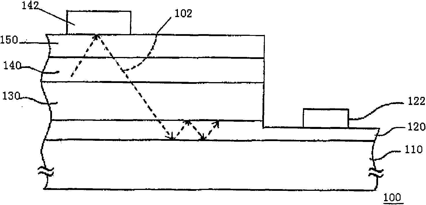
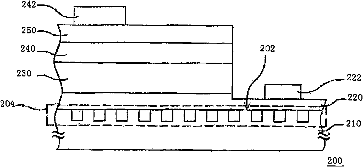
[0022] figure 2 It is a schematic cross-sectional view of the light-emitting diode structure of the present invention. Please refer to figure 2 The light emitting diode structure 200 is mainly composed of a substrate 210, a first type doped semiconductor layer 220, an electrode 222, a light emitting layer 230, a second type doped semiconductor layer 240, and an electrode 242. The material of the substrate 210 is, for example, silicon, sapphire, silicon carbide or spinel, and the substrate 210 has a surface 202 and a plurality of cylindrical photonic crystals 204 on the surface 202.

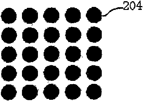
[0023] As mentioned above, the photonic crystals 204 are, for example, convex patterns or grooves, and the method of forming these photonic crystals 204 is, for example, to perform photolithography and etching processes on the substrate 210 to form cylindrical convex patterns or grooves on the surface 202 thereof. Groove. In particular, the photonic crystals 204 are periodically arranged on the su...


PUM

PropertyMeasurementUnit
Diameteraaaaaaaaaa

Abstract

The invention discloses a light-emitting diode (LED) structure which comprises a substrate, a first doped semiconductor layer, a first electrode, a light-emitting layer, a second doped semiconductor layer and a second electrode, wherein the substrate is provided with a surface and a plurality of cylindrical photon crystals positioned on the surface; the first doped semiconductor layer is arranged on the substrate to cover the photon crystals; the light-emitting layer, the second doped semiconductor layer and the second electrode are sequentially arranged on part of the first doped semiconductor layer; and the first electrode is arranged on part of the first doped semiconductor layer on which the light-emitting layer is not covered. Because the substrate provided with the photon crystals can improve the epitaxial quality of the first doped semiconductor layer and increase the light energy of the forward ejected LED structure, the light-emitting efficiency of the LED structure can be effectively improved.

Description

technical field [0001] The invention relates to a light emitting element, in particular to a light emitting diode structure. Background technique [0002] Compared with traditional lamps, light-emitting diodes have absolute advantages, such as small size, long life, low voltage / current drive, not easy to break, no significant heat problems when emitting light, no mercury (no pollution problems), good luminous efficiency ( Power-saving) and other characteristics, and the luminous efficiency of light-emitting diodes has been continuously improved in recent years, so light-emitting diodes have gradually replaced fluorescent lamps and incandescent bulbs in some fields, such as scanner light sources that require high-speed response, backlights for liquid crystal displays or Dashboard lighting, traffic lights, and general lighting devices for front light vehicles. [0003] Moreover, since the nitrogen-containing III-V compound is a material with a wide band energy gap, its lumine...

Claims


Application Information

Patent Timeline
IPC IPC(8): H01L33/00
Inventor 武良文蔡亚萍简奉任
Owner 江苏璨扬光电有限公司
Why Eureka
Try Eureka