Semiconductor light-emitting device with selectively formed buffer layer on substrate

a technology of semiconductor light-emitting device and substrate, which is applied in the manufacture of semiconductor/solid-state devices, semiconductor devices, electrical devices, etc., to achieve the effects of enhancing the external quantum efficiency reducing the total reflection, and increasing the epitaxy quality of the semiconductor light-emitting devi

Inactive Publication Date: 2009-02-26
SINO AMERICAN SILICON PROD +1
View PDF6 Cites 2 Cited by
  • Summary
  • Abstract
  • Description
  • Claims
  • Application Information

AI Technical Summary

Benefits of technology

[0015]Compared to the prior art, the buffer layer of the semiconductor light-emitting device according to the invention is selectively formed on the substrate and is for scattering light emitted from the semiconductor light-emitting device to reduce the total reflection and further enhance the external quantum efficiency of the semiconductor light-emitting device. Furthermore, the buffer layer can assist a bottom-most layer of the multi-layer structure in lateral and vertical epitaxial growth to increase the epitaxy quality of the semiconductor light-emitting device.
[0016]The advantage and spirit of the invention may be understood by the following recitations together with the appended drawings.

Problems solved by technology

One of the main causes for such losses is the high refractive index of the semiconductor material so the radiation cannot be emitted outside at the semiconductor surface on account of total reflection.

Method used


Image

  • Semiconductor light-emitting device with selectively formed buffer layer on substrate
  • Semiconductor light-emitting device with selectively formed buffer layer on substrate
  • Semiconductor light-emitting device with selectively formed buffer layer on substrate

Examples


Embodiment Construction

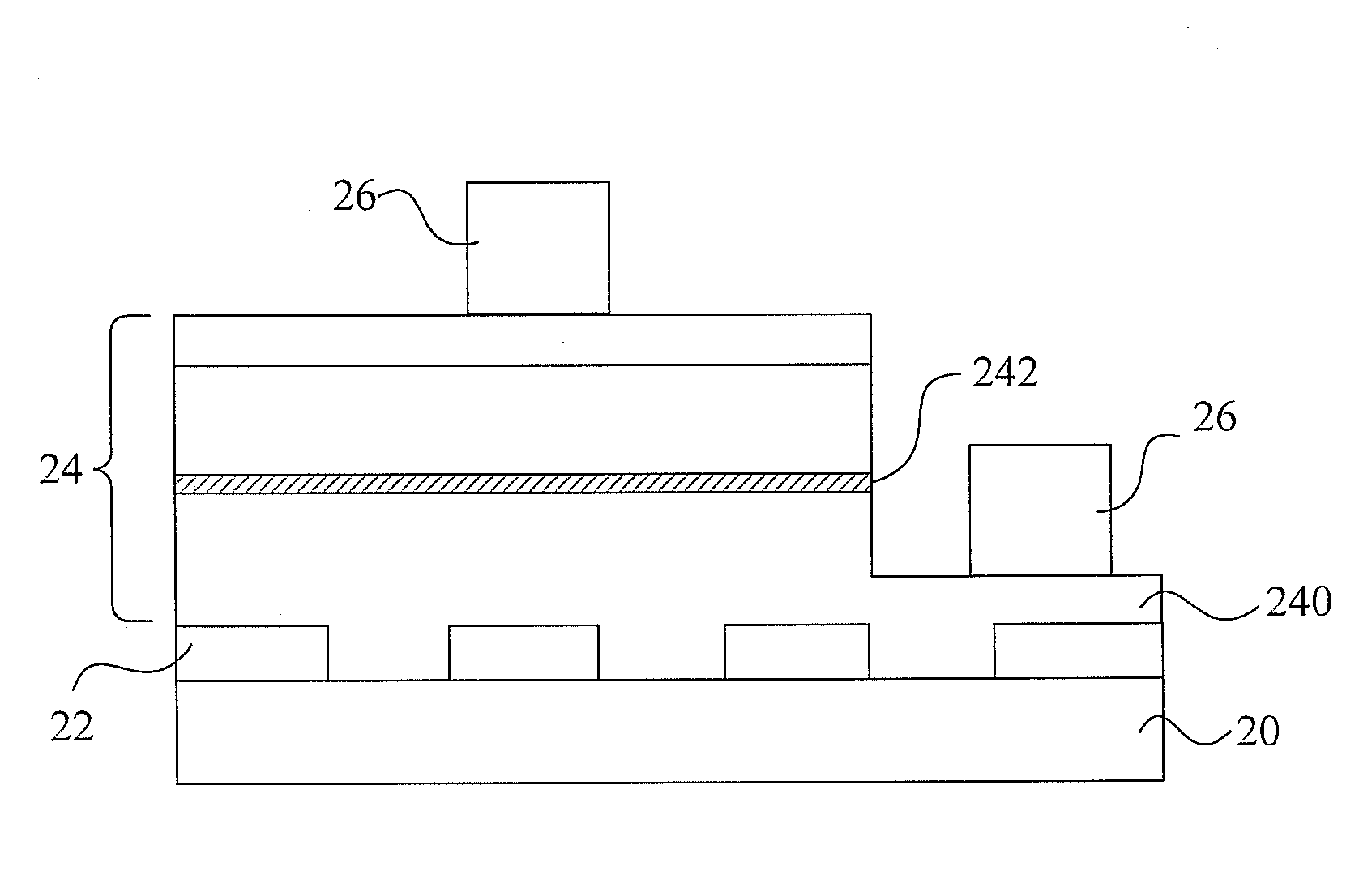
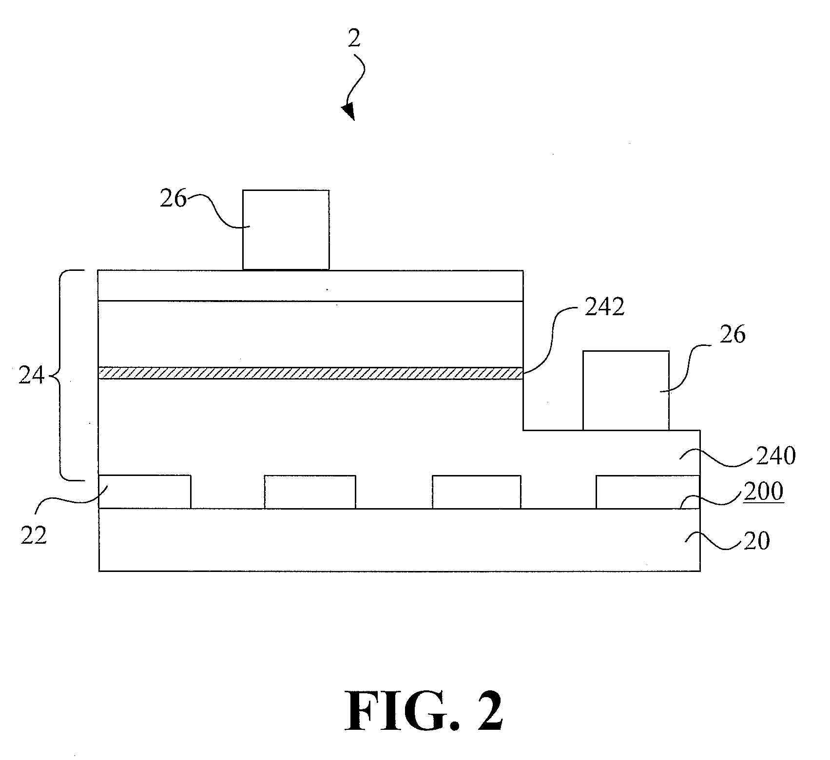
[0020]Please refer to FIG. 2. FIG. 2 illustrates a sectional view of a semiconductor light-emitting device 2 according to an embodiment of the invention. As shown in FIG. 2, the semiconductor light-emitting device 2 includes a substrate 20, a buffer layer 22, a multi-layer structure 24, and an ohmic electrode structure 26.

[0021]In practical applications, the substrate 20 can be made of sapphire, Si, SiC, GaN, ZnO, ScAlMgO4, YSZ (Yttria-Stabilized Zirconia), SrCu2O2, LiGaO2, LiAlO2, GaAs and the like.

[0022]The buffer layer 22 is selectively formed on an upper surface 200 of the substrate 20 such that the upper surface 200 of the substrate 20 is partially exposed. The multi-layer structure 24 is formed to overlay the buffer layer 22 and the exposed upper surface 200 of the substrate 20. The multi-layer structure 24 includes a light-emitting region 242. The buffer layer 22 is formed to assist a bottom-most layer 240 of the multi-layer structure 24 in lateral and vertical epitaxial grow...


PUM


Abstract

The invention discloses a semiconductor light-emitting device and a method of fabricating the same. The semiconductor light-emitting device according to the invention includes a substrate, a buffer layer, a multi-layer structure, and an ohmic electrode structure. The buffer layer is selectively formed on an upper surface of the substrate such that the upper surface of the substrate is partially exposed. The multi-layer structure is formed to overlay the buffer layer and the exposed upper surface of the substrate. The multi-layer structure includes a light-emitting region. The buffer layer assists a bottom-most layer of the multi-layer structure in lateral and vertical epitaxial growth. The ohmic electrode structure is formed on the multi-layer structure.

Description

BACKGROUND OF THE INVENTION[0001]1. Field of the Invention[0002]The present invention relates to a semiconductor light-emitting device and, more particularly, to a semiconductor light-emitting device with an enhanced external quantum efficiency and a good epitaxy quality.[0003]2. Description of the Prior Art[0004]The current semiconductor light-emitting devices, such as light-emitting diodes, have been used for a wide variety of applications, e.g. illuminations and remote controls. To ensure high functional reliability as great as possible and a low power requirement of the semiconductor light-emitting devices, the external quantum efficiency is required for the devices.[0005]In principle, the external quantum efficiency of a semiconductor light-emitting device is determined both by the internal quantum efficiency and extraction efficiency. The internal quantum efficiency is determined by the material property and quality. The extraction efficiency refers to the proportion of radiat...

Claims


Application Information

Patent Timeline
Patent Type & Authority Applications(United States)
IPC IPC(8): H01L33/00H01L33/12
CPCH01L33/12H01L33/007
Inventor CHEN, MIIN-JANGHSU, WEN-CHINGHO, SZU-HUA
Owner SINO AMERICAN SILICON PROD
Why Eureka
Try Eureka