High-quality silicon carbide epitaxial growth technology

A high-quality silicon carbide, epitaxial growth technology, applied in the direction of single crystal growth, crystal growth, single crystal growth, etc., can solve the problems of epitaxial quality reduction, inability to completely eliminate substrate propagation, etc., and achieve improved characteristics and yield, reproducible Highly flexible and controllable effects

Inactive Publication Date: 2018-03-23
EPIWORLD INT
View PDF3 Cites 3 Cited by
  • Summary
  • Abstract
  • Description
  • Claims
  • Application Information

AI Technical Summary

Problems solved by technology

[0004] However, in the above-mentioned epitaxial process, since there are only two interfaces between the substrate and the buffer layer, and the buffer layer and the epitaxial layer in the whole epitaxial growth process, there are many dislocation defects in the silicon carbide substrate, such as threading screw dislocation defects, penetrating Edge dislocation defects and basal layer fault defects, etc., because the epitaxial growth of silicon carbide is homoepitaxial growth, the above two interfaces cannot completely eliminate the propagation of defects in the substrate to the epitaxial layer, so the dislocation defects in the substrate will be As the growth extends to the epitaxial layer, there are still a certain number of defects in the epitaxial layer, resulting in a decrease in the quality of the epitaxial layer

Method used


Image

  • High-quality silicon carbide epitaxial growth technology
  • High-quality silicon carbide epitaxial growth technology

Examples


Embodiment 1

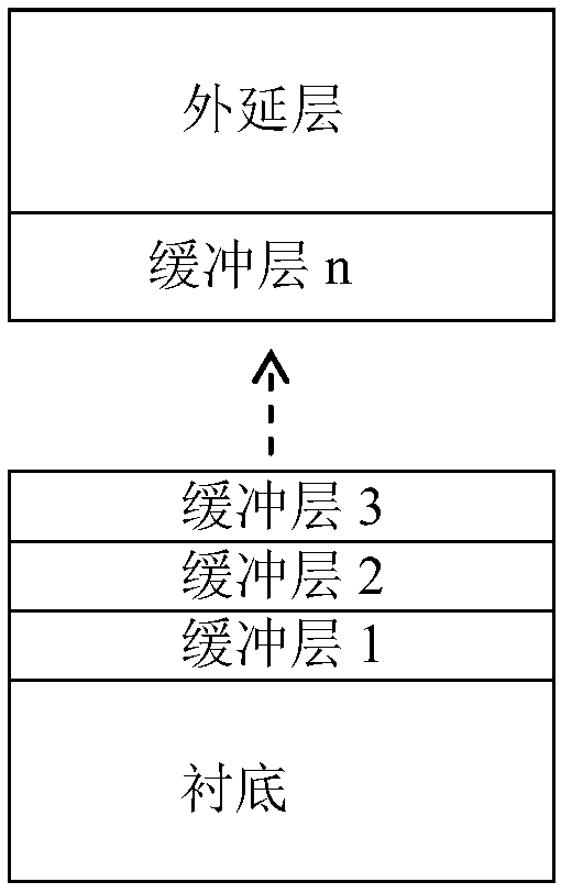
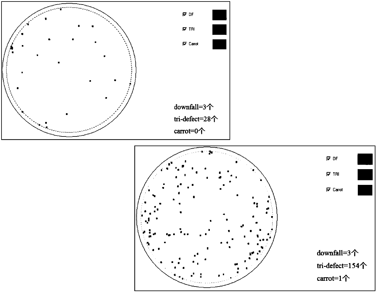
[0025] Provides a nitrogen doping concentration of 1 x 10 18 atoms / cm 3 SiC substrate, 2 layers grown by CVD with a nitrogen doping concentration of 1×10 18 atoms / cm 3 buffer layer, wherein: the growth rate of the first layer is 5 μm / h, and the thickness is 0.5 μm; the growth rate of the second layer is 10 μm / h, and the thickness is 0.5 μm. Then grow on the uppermost buffer layer with a nitrogen doping concentration of 1×10 16 atoms / cm 3 The epitaxial layer, the growth rate of the epitaxial layer is 15 μm / h, and the thickness is 10 μm. As a comparative example, a single buffer layer with a thickness of 10 μm was continuously grown on the above-mentioned SiC substrate at a growth rate of 5 μm / h and then an epitaxial layer was grown, and other control conditions were the same. Detect the defect distribution situation of the epitaxial wafer of embodiment 1 and comparative example, see figure 1 , Visible defects are significantly reduced, improving the epitaxial quality.


PUM

PropertyMeasurementUnit
thicknessaaaaaaaaaa
thicknessaaaaaaaaaa

Abstract

The invention discloses a high-quality silicon carbide epitaxial growth technology. A plurality of silicon carbide buffer layers are sequentially homogeneously grown on a silicon carbide substrate bya chemical vapor deposition process, and a silicon carbide epitaxial layer is grown on the uppermost buffer layer, wherein the growth rate of all the buffer layers increases stepwise from bottom to top, and the growth rate of the top buffer layer is not higher than the growth rate of the epitaxial layer. Multiple buffer layers are formed through the stepped control of the growth rate, and a plurality of interfaces formed by the brief growth interruption among the buffer layers sequentially reduce the propagation of defects, so the extended propagation of the defects of the substrate to the epitaxial layer is blocked, the number of the defects in the epitaxial layer is reduced, the epitaxial quality is improved, and the characteristics and the yield of functional devices manufactured basedon above obtained epitaxial wafers are improved.

Description

technical field [0001] The invention relates to semiconductor manufacturing technology, in particular to a high-quality silicon carbide epitaxial growth process. Background technique [0002] Silicon carbide semiconductor has excellent characteristics such as large bandgap width, excellent stability, high thermal conductivity, high critical breakdown field strength, high saturation electron drift velocity, etc. It is the best choice for making high temperature, high frequency, high power and strong radiation power electronic devices ideal semiconductor material. Compared with traditional silicon devices, silicon carbide devices can work normally under the electric field strength 10 times that of silicon devices. The silicon carbide material used to make silicon carbide devices is usually a silicon carbide epitaxial wafer grown on a silicon carbide substrate. [0003] At present, the epitaxial growth of silicon carbide has been commercialized, and the method of CVD (chemica...

Claims


Application Information

Patent Timeline
Patent Type & Authority Applications(China)
IPC IPC(8): C30B25/18C30B29/36
CPCC30B25/183C30B29/36
Inventor 钱卫宁冯淦赵建辉
Owner EPIWORLD INT
Why Eureka
Try Eureka