

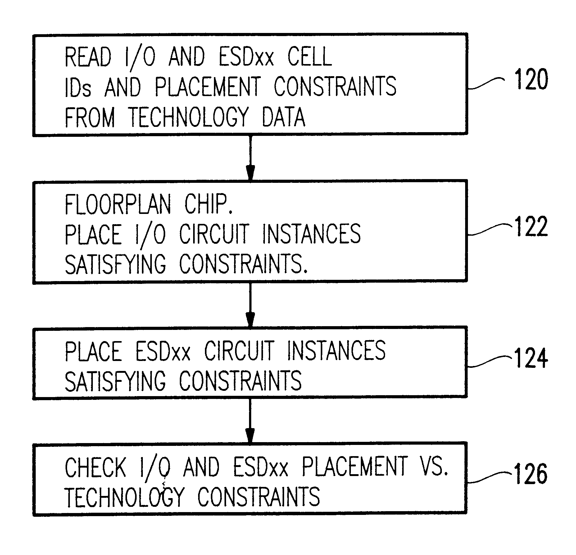
Method of automated design and checking for ESD robustness
- Summary
- Abstract
- Description
- Claims
- Application Information
AI Technical Summary
Problems solved by technology
Method used
Image

Examples
Embodiment Construction
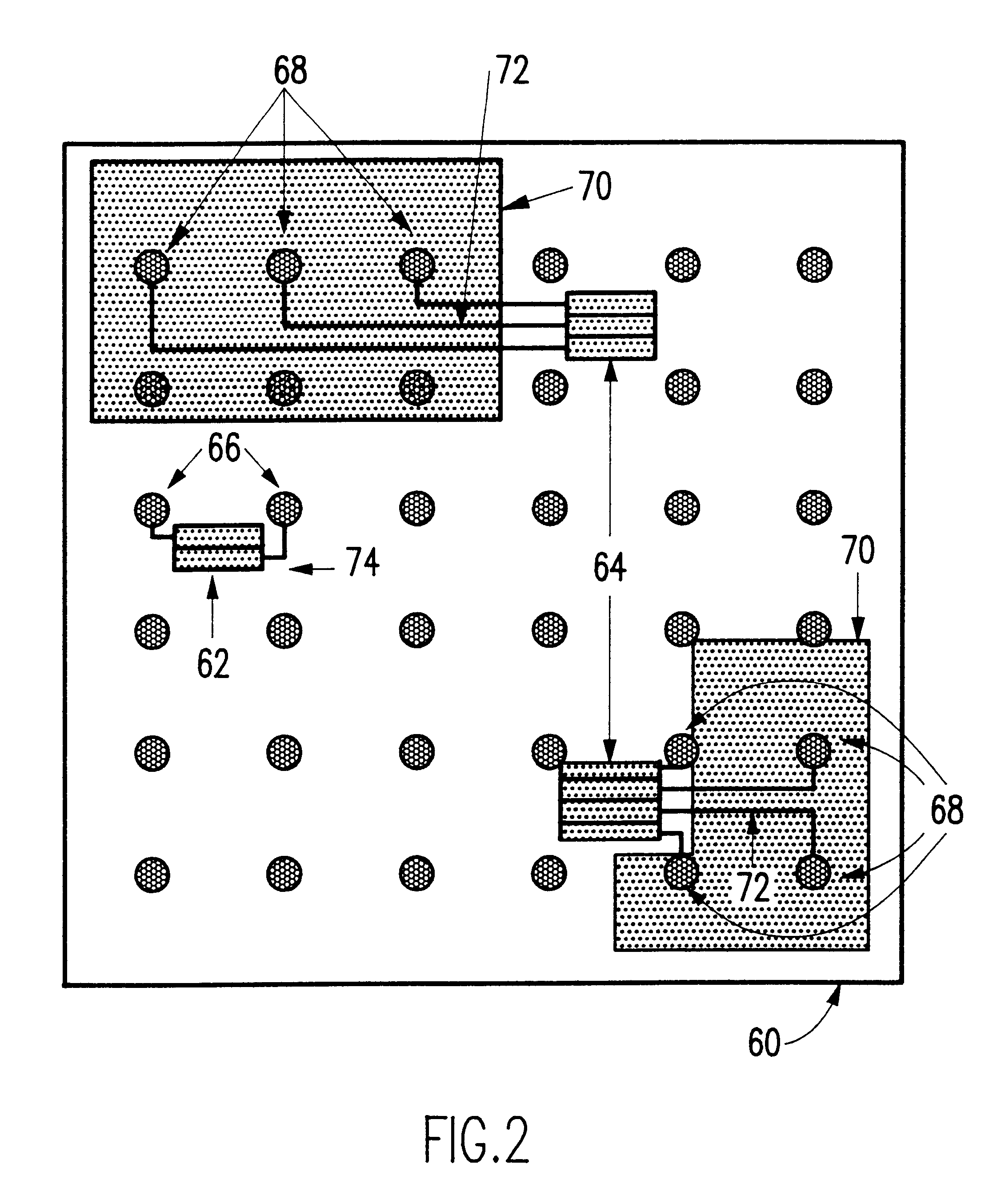
Referring now to FIG. 2, which shows a pad array chip 60 designed according to the preferred embodiment method to provide robust I / O and power connections. I / O circuits instances 62, 64 may be located throughout the chip 60 and are connected to pads 66, 68. Pads 68 are located over core circuit areas 70. Nets 72 between I / O cell instances 64 and pads 68 and nets 74 between I / O cell instances 62 and pads 66 having been formed according to the preferred embodiment design method have robust ESD protection.
According to the preferred embodiment method, each I / O instance 62, 64 includes an ESD protect device and connection between the ESD device therein and the cell's active circuitry. Thus, the preferred embodiment method is intended for IC chips 60 where power distribution is a mesh of wires on several conductive (metal) levels. The mesh is modifiable to allow the addition of large circuit blocks, sometimes referred to as megacells or large memory bocks. Each power supply is represented...
PUM
 Abstract
Description
Claims
Application Information