
Integrated metal-insulator-metal capacitor and metal gate transistor

a metal-insulator, metal-gate transistor technology, applied in the direction of diodes, semiconductor devices, electrical apparatus, etc., can solve the problems of increasing process cost and difficult reduction

Inactive Publication Date: 2004-09-07
INT BUSINESS MASCH CORP
View PDF10 Cites 26 Cited by
  • Summary
  • Abstract
  • Description
  • Claims
  • Application Information

AI Technical Summary

Benefits of technology

The planarizing of the first metal layer reduces voids and surface irregularities in the second metal layer. The insulator comprises both a capacitor insulator and a gate insulator. In addition, after forming the sidewall spacers, the invention dopes source and drain regions in the substrate.

Problems solved by technology

Unlike conventional stand-alone DRAMs, the size of erasable DRAM (eDRAM) is more difficult to reduce, which increases the process cost.

Method used


Image

  • Integrated metal-insulator-metal capacitor and metal gate transistor
  • Integrated metal-insulator-metal capacitor and metal gate transistor
  • Integrated metal-insulator-metal capacitor and metal gate transistor

Examples


Embodiment Construction

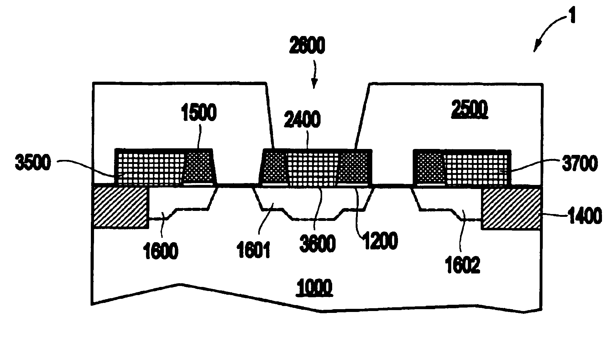
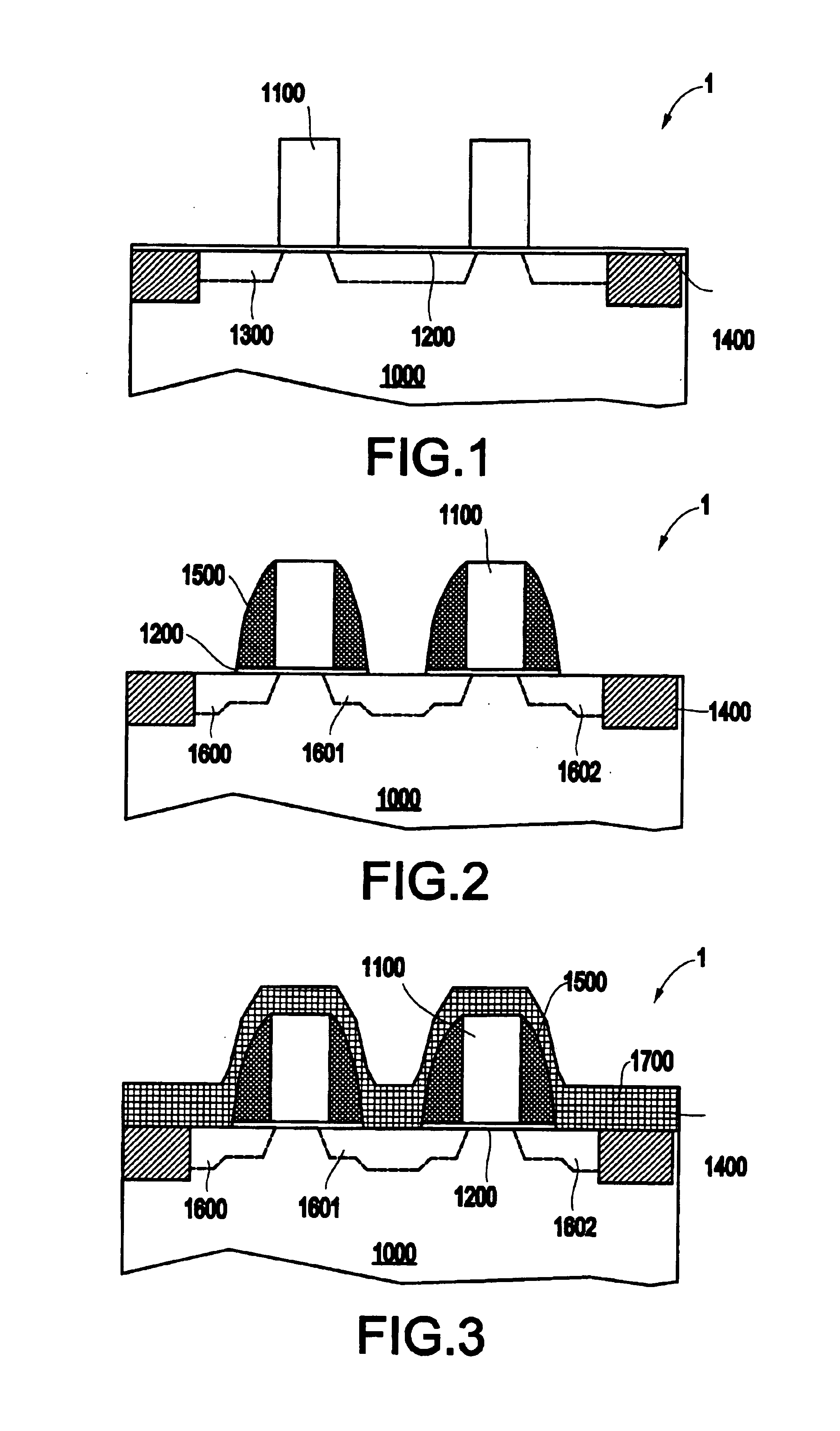
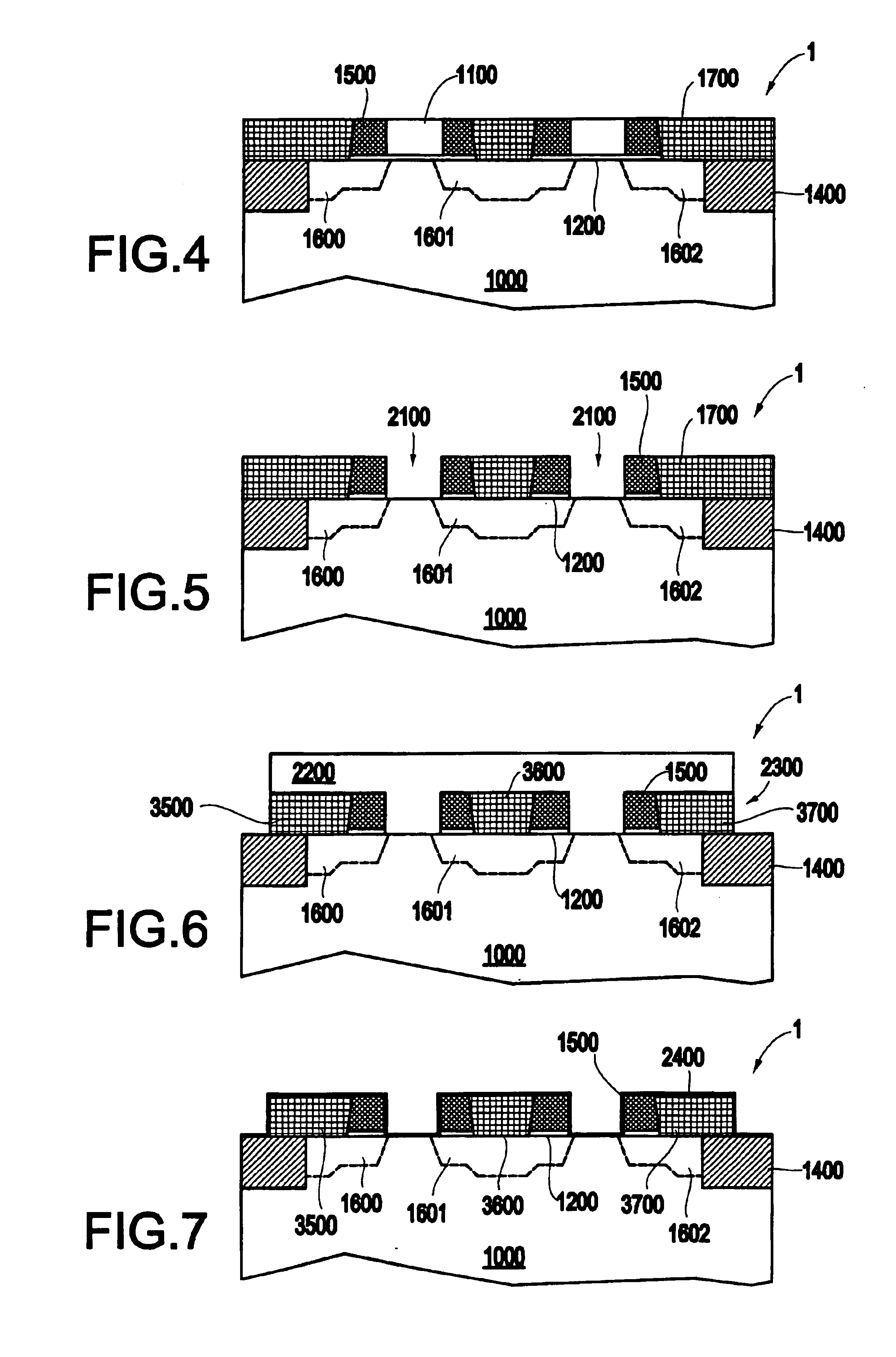
For eDRAM, not only must the performance of DRAM be improved, but the performance of the other logic circuits, such as the CPU, must also be improved for overall system performance to improve. The current trend of using a metal gate for both the DRAM and support circuits for embedded applications is well known. Using a metal capacitor (such as a MIM) for the DRAM and support circuits saves chip size, especially when a high-k dielectric material is incorporated. High-k (dielectric constant) materials such as aluminum oxide, tantalum pentoxide, titanium dioxides, barium strontium titanate, or other ferroelectric materials are compatible with metal plates. The following describes a process to form a metal gate and metal contact capacitor side-by-side in a DRAM cell configuration. However, the embodiment shown below is merely exemplary and, as would be known by one ordinarily skilled in the art, the invention is equally applicable to other structures such as support circuits where a cap...


PUM


Abstract

An integrated circuit structure is disclosed that comprises a pair of capacitors, each having metal plates separated by an insulator, and metal gate semiconductor transistors electrically connected to the capacitors. The metal gate of the transistors and one of the metal plates of each of the capacitors comprise the same metal level in the integrated circuit structure. More specifically, each of the capacitors comprise a vertical capacitor having an upper metal plate vertically over a lower metal plate and each metal gate of the transistors and each upper metal plate of the capacitors comprise the same metal level in the integrated circuit structure.

Description

1. Field of the InventionThe present invention generally relates to microelectronic circuits, and more particularly to a microelectronic circuit and device having metal-insulator-metal capacitors.2. Description of the Related ArtIn today's dynamic random access memory (DRAM) environment, achieving high density is of the utmost concern. As the DRAM size continues to grow larger, its performance becomes a concern. Therefore, it is critical to improve the performance of the DRAM, especially for short-cycle, high-speed embedded DRAMs. In order to compete with the technological embodiments of static random access memories (SRAMs), there are many performance breakthroughs which must occur to the DRAMs. One such breakthrough is to further reduce the DRAM size. The size of a DRAM macro is about 10 to 15 times smaller than that of SRAM with the same capacity. Moreover, the smaller the size, the less the delay. Unlike conventional stand-alone DRAMs, the size of erasable DRAM (eDRAM) is more d...

Claims


Application Information

Patent Timeline
Patent Type & Authority Patents(United States)
IPC IPC(8): H01L21/336H01L21/28H01L21/02H01L29/423H01L29/40H01L29/49H01L27/06H01L29/51H01L27/10H01L21/8242H01L27/108
CPCH01L21/28079H01L29/66545H01L21/28114H01L21/28194H01L27/0629H01L27/10805H01L27/1085H01L29/42376H01L29/495H01L29/4958H01L29/4966H01L29/517H01L21/28088H01L27/10885H01L29/51H10B12/30H10B12/03H10B12/482H10B12/00
Inventor CLEVENGER, LAWRENCE A.HSU, LOUIS L.WONG, KWONG HON
Owner INT BUSINESS MASCH CORP
Learn More