Substrate structure of flip chip package

a flip chip and substrate technology, applied in the direction of printed circuit assembling, printed circuit manufacturing, printed circuit aspects, etc., can solve the problems of relatively small process tolerance, reduced packaging density, and relatively difficult layout work of the substrate of the flip chip packag

Inactive Publication Date: 2004-09-07
SILICONWARE PRECISION IND CO LTD
View PDF6 Cites 134 Cited by
  • Summary
  • Abstract
  • Description
  • Claims
  • Application Information

AI Technical Summary

Problems solved by technology

But the collapse phenomenon of the SMD and the bondability (between the bump and the mounting pad) are poor, thereby, the demand for the coplanarity of the substrate of the flip chip package is relatively rigorous, and the process tolerance is relatively small.
As a result, the pitch of the mounting pads needed to be increased to meet this requirement, thus the packaging density becomes lower, and this makes the layout work of the substrate of the flip chip package relatively difficult.
But based on the limitation of the fabrication and design ability, the disposition of the contact points is limited.

Method used


Image

  • Substrate structure of flip chip package
  • Substrate structure of flip chip package
  • Substrate structure of flip chip package

Examples


Embodiment Construction

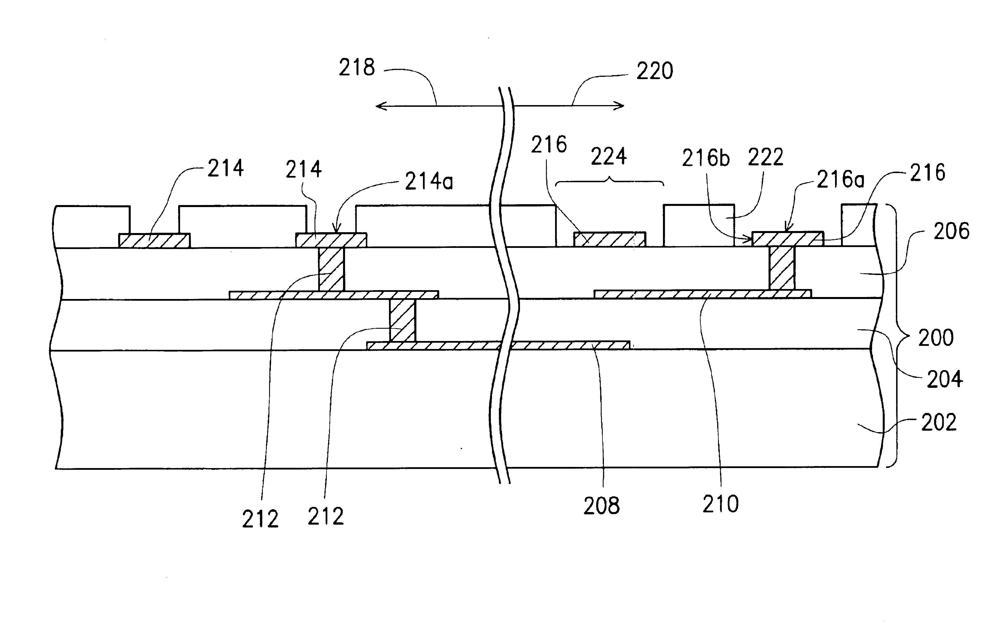
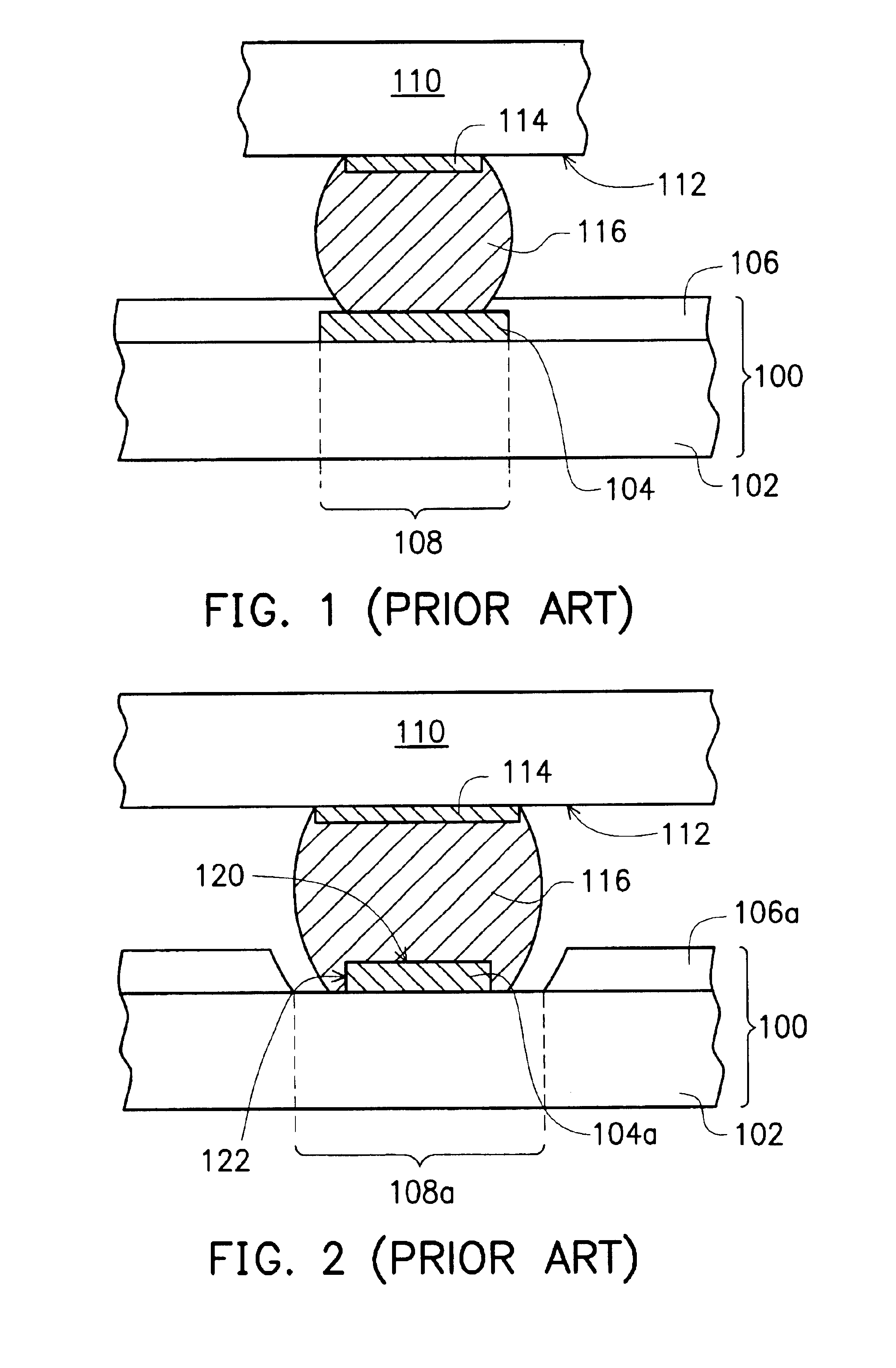
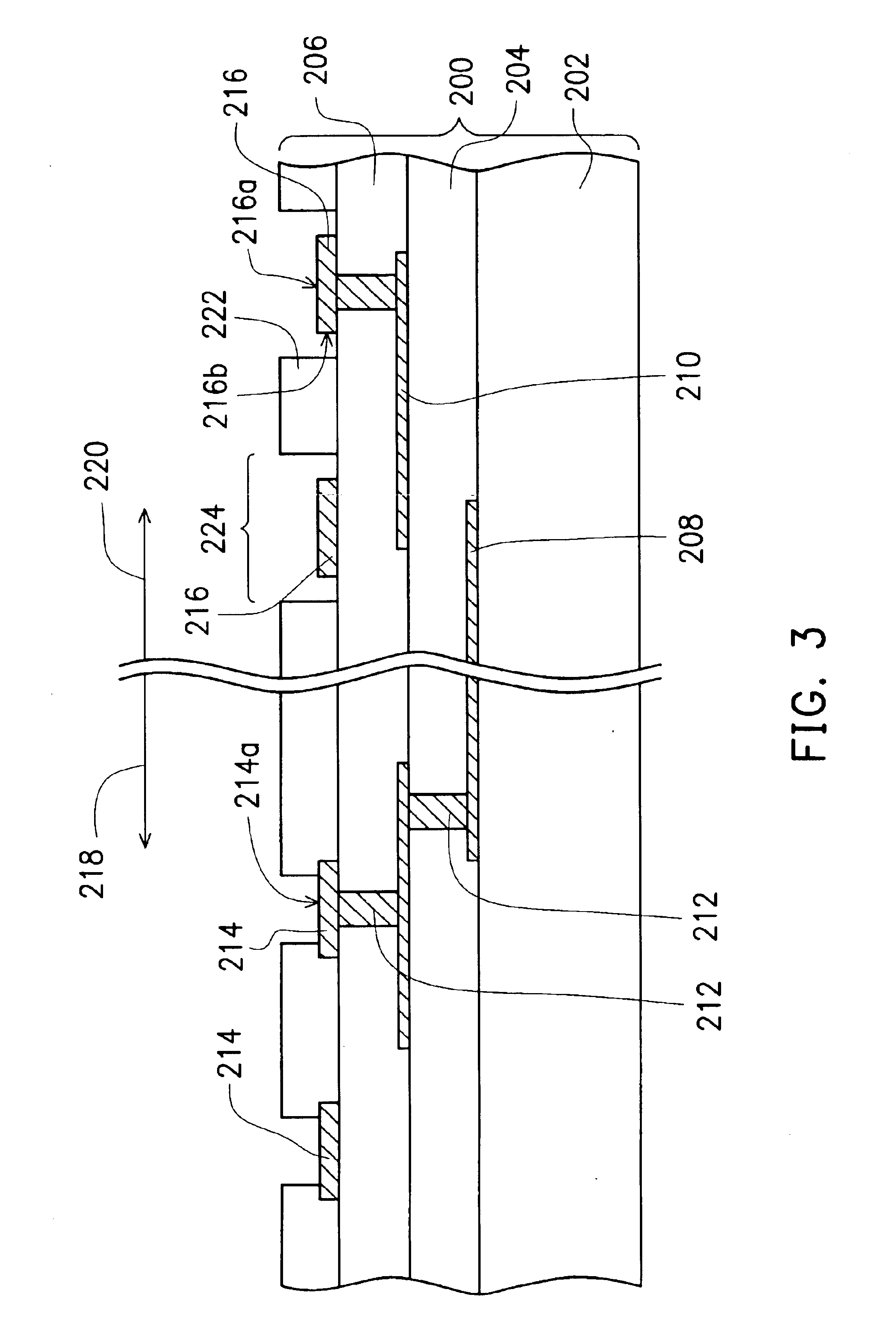
FIG. 3 shows a cross-sectional view of a substrate structure of a flip chip package according to a preferred embodiment of the present invention, and FIG. 4 shows a top view of a substrate structure of a flip chip package according to a preferred embodiment of the present invention. As shown in FIG. 3 and FIG. 4, a substrate 200 of a flip chip package of the present invention is mainly constituted by alternately stacking up a multiplicity of insulative layers 202, 204, 206 and a multiplicity of patterned circuit layers 208, 210. Among them, the insulative layer 202 is an insulative layer that is made of "flame-retardant epoxy-glass fabric composite resin " or Bismaleimide-Taiazine (BT) etc. The material for the insulative layer 204, 206 is the one such as epoxy. The patterned circuit layer 208, 210 being made of copper foil and defined by photolithographic and etching processes forms electrical connection through a via 212 in the insulative layer 204, 206. The patterned circuit laye...


PUM


Abstract

A substrate structure of Flip Chip package includes a plurality of patterned circuit layers alternately stacking up with at least an insulative layer for isolating the patterned circuit layers. The patterned circuit layers are electrically connected each other wherein one of the patterned circuit layers is positioned on the surface of the substrate. The patterned circuit layer includes a plurality of first mounting pads and a plurality of second mounting pads. The solder mask layer covers the patterned circuit layer on the surface of the substrate, and a portion of the surface of the outer edge of the mounting pads while exposes a portion of the surface of the first mounting pads and the whole surface of the second mounting pads.

Description

1. Field of the InventionThis invention relates to a substrate structure of flip chip package, and more particularly to a substrate structure of flip chip package that can improve the bondability of the bump.2. Description of Related ArtThe Flip Chip technology being a package technology frequently applied in the CSP (Chip Scale Technology) can diminish the packaging area and shorten the path of signal transmission through the bump attachment to a carrier since the Flip Chip technology can employ area array for the disposition of bonding pads. In the current Flip Chip products, the contact area between the bump and the mounting pad can be changed, thereby, the collapse phenomenon will be affected depending on the extent of coverage of the solder mask over the mounting pad. The conventional mounting pad design can be classified into two categories, that is, SMD (Solder Mask Define) and NSMD (Non Solder Mask Define).FIG. 1 shows the mounting pad structure of SMD according to a prior a...

Claims


Application Information

Patent Timeline
Patent Type & Authority Patents(United States)
IPC IPC(8): H01L21/56H01L23/48H01L23/498H01L21/02H05K3/34
CPCH01L21/563H01L23/49894H05K3/3452H01L2224/13021H01L2224/73203H05K3/3436H05K2201/094H05K2201/0989H05K2201/099H05K2201/10674H05K2201/10977H01L2924/01087H01L2224/16225H01L2224/32225H01L2224/73204H01L2924/00H01L2224/05573H01L2224/05568H01L2224/056H01L24/17H01L2224/16237H01L2224/16238H01L2224/17104H01L2224/1703H01L24/16H01L2224/06131H01L2924/00014
Inventor TSAI, YING-CHOUPU, HAN-PINGCHIU, SHIH-KUANG
Owner SILICONWARE PRECISION IND CO LTD
Why Eureka
Try Eureka