Use of printing and other technology for micro-component placement

a technology of micro-components and printing, applied in the field of lightemitting panels, can solve the problems of high cost of ito, high cost of final plasma display, and high cost of manufacturing process and ultimately final plasma display

Inactive Publication Date: 2004-09-28
LEIDOS
View PDF157 Cites 60 Cited by
  • Summary
  • Abstract
  • Description
  • Claims
  • Application Information

AI Technical Summary

Benefits of technology

Further, the light-emitting panel may be used in flat-panel displays. These displays can be manufactured very thin and lightweight, when compared to similar sized cathode ray tube (CRTs), making them ideally suited for home, office, theaters and billboards. In addition, these displays can be manufactured in large sizes and with sufficient resolution to accommodate high-definition television (HDTV). Gas-plasma panels do not suffer from electromagnetic distortions and are, therefore, suitable for applications strongly affected by magnetic fields, such as military applications, radar systems, railway stations and other underground systems.
Another embodiment of the present invention includes a method for depositing a plurality of micro-components onto predetermined portions of a substrate. This method includes charging a first predetermined portion of the substrate with a first charge; charging a first set of the plurality of micro-components with a second charge, wherein the first charge and the second charge are opposite charges; introducing the first set of charged micro-components to the first charged portion of the substrate wherein the first set of charged micro-components is electrostatically attracted to the first charged portion of the substrate; facilitating removal of micro-components from the first set of charged micro-components that did not adhere to the first charged portion of the substrate by means of a force applied to the substrate; charging a second predetermined portion of the substrate with the first charge; charging a second set of the plurality of micro-components with the second charge, wherein the first charge and the second charge are opposite charges; introducing the second set of charged micro-components to the second charged portion of the substrate wherein the second set of charged micro-components is electrostatically attracted to the second charged portion of the substrate; applying a force to the substrate in order to remove micro-components from the second set of charged micro-components that did not adhere to the second charged portion of the substrate; charging a third predetermined portion of the substrate with the first charge; charging a third set of the plurality of micro-components with the second charge, wherein the first charge and the second charge are opposite charges; introducing the third set of charged micro-components to the third charged portion of the substrate wherein the third set of charged micro-components is electrostatically attracted to the third charged portion of the substrate; and applying a force to the substrate in order to remove micro-components from the third set of charged micro-components that did not adhere to the third charged portion of the substrate.
Another embodiment of the present invention includes a method for placing micro-components into the sockets of a substrate. This method includes placing a first mask having first holes in predetermined locations over the substrate, wherein the first holes are positioned over a first set of sockets within the substrate; introducing multiple micro-components for emitting a first color to the mask; applying a force to at least one of the first mask and the substrate in order to facilitate placement of the micro-components into the first set of sockets within the substrate; placing a second mask having second holes in predetermined locations over the substrate, wherein the second holes are positioned over a second set of sockets within the substrate; introducing multiple micro-components for emitting a second color to the mask; applying a force to at least one of the second mask and the substrate in order to facilitate placement of the micro-components into the second set of sockets within the substrate; placing a third mask having third holes in predetermined locations over the substrate, wherein the third holes are positioned over a third set of sockets within the substrate; introducing multiple micro-components for emitting a third color to the mask; and applying a force to at least one of the third mask and the substrate in order to facilitate placement of the micro-components into the third set of sockets within the substrate.

Problems solved by technology

Using ITO, however, has several disadvantages, for example, ITO is expensive and adds significant cost to the manufacturing process and ultimately the final plasma display.
The sealing of the outer edges of the parallel plates and the introduction of the plasma forming gas are both expensive and time-consuming processes, resulting in a costly end product.
In addition, it is particularly difficult to achieve a good seal at the sites where the electrodes are fed through the ends of the parallel plates.
This can result in gas leakage and a shortened product lifecycle.
Another disadvantage is that individual pixels are not segregated within the parallel plates.
As a result, gas ionization activity in a selected pixel during a write operation may spill over to adjacent pixels, thereby raising the undesirable prospect of possibly igniting adjacent pixels.
In addition, in this type of display panel it is difficult to properly align the electrodes and the gas chambers, which may cause pixels to misfire.
As with the open display structure, it is also difficult to get a good seal at the plate edges.
Furthermore, it is expensive and time consuming to introduce the plasma producing gas and seal the outer edges of the parallel plates.
Long cycle times increase product cost and are undesirable for numerous additional reasons known in the art.
For example, a sizeable quantity of substandard, defective, or useless fully or partially completed plasma panels may be produced during the period between detection of a defect or failure in one of the components and an effective correction of the defect or failure.
Consequently, the display can only be tested after the two parallel plates are sealed together and the plasma-forming gas is filled inside the cavity between the two plates.

Method used


Image

  • Use of printing and other technology for micro-component placement
  • Use of printing and other technology for micro-component placement
  • Use of printing and other technology for micro-component placement

Examples


Embodiment Construction

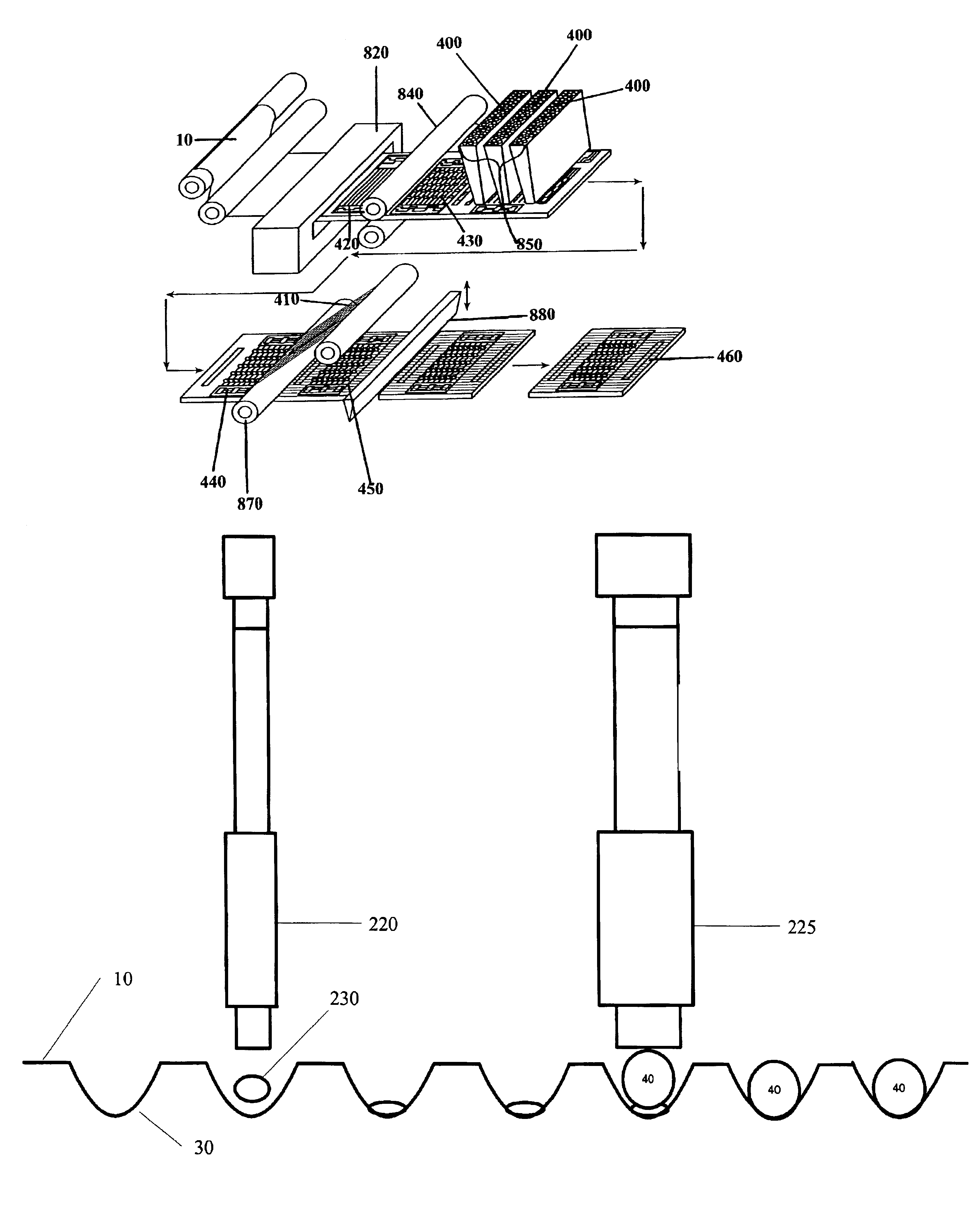
As embodied and broadly described herein, the preferred embodiments of the present invention are directed to a novel light-emitting panel. In particular, preferred embodiments are directed to light-emitting panels and to a web fabrication process for manufacturing light-emitting panels.

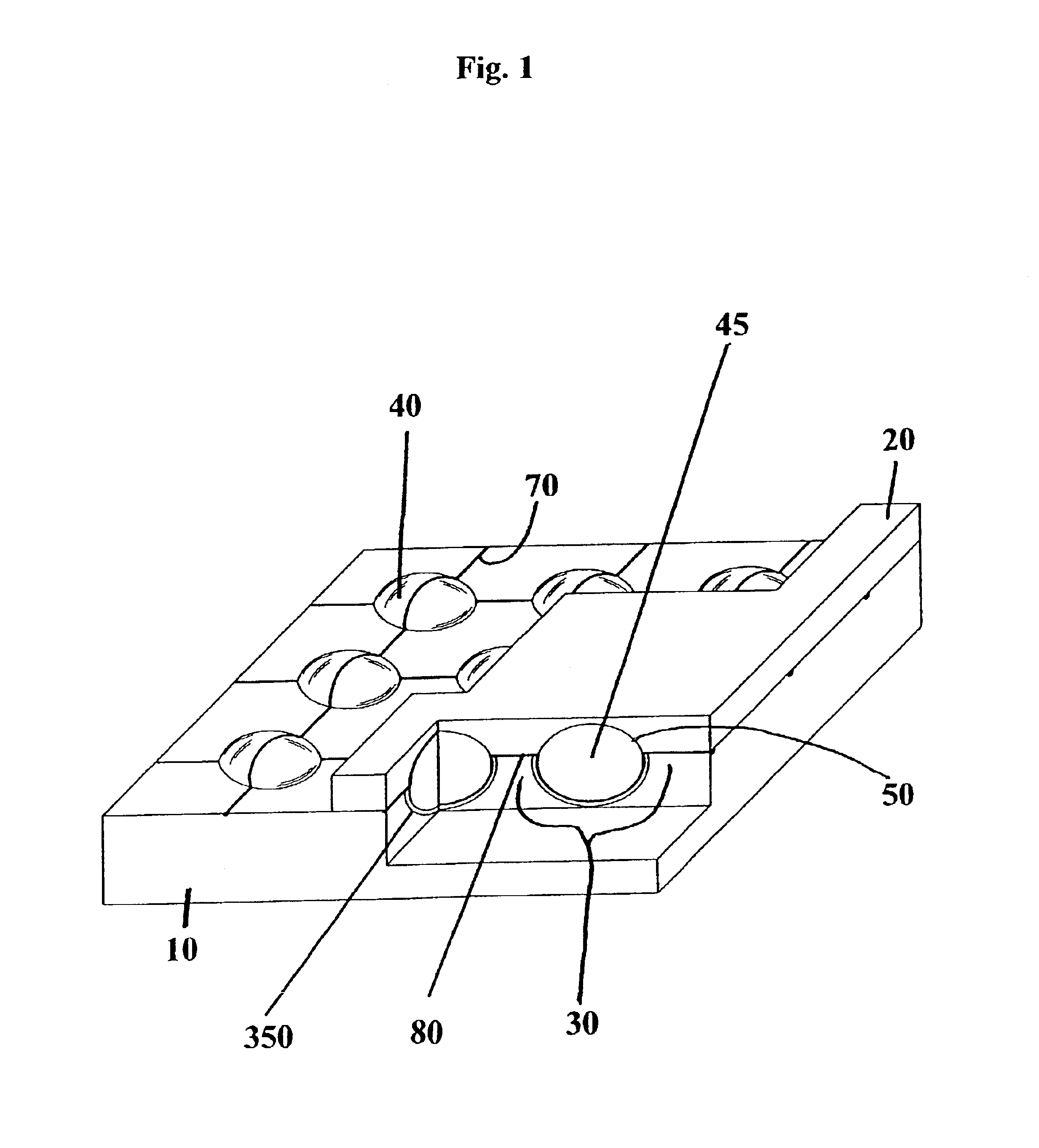
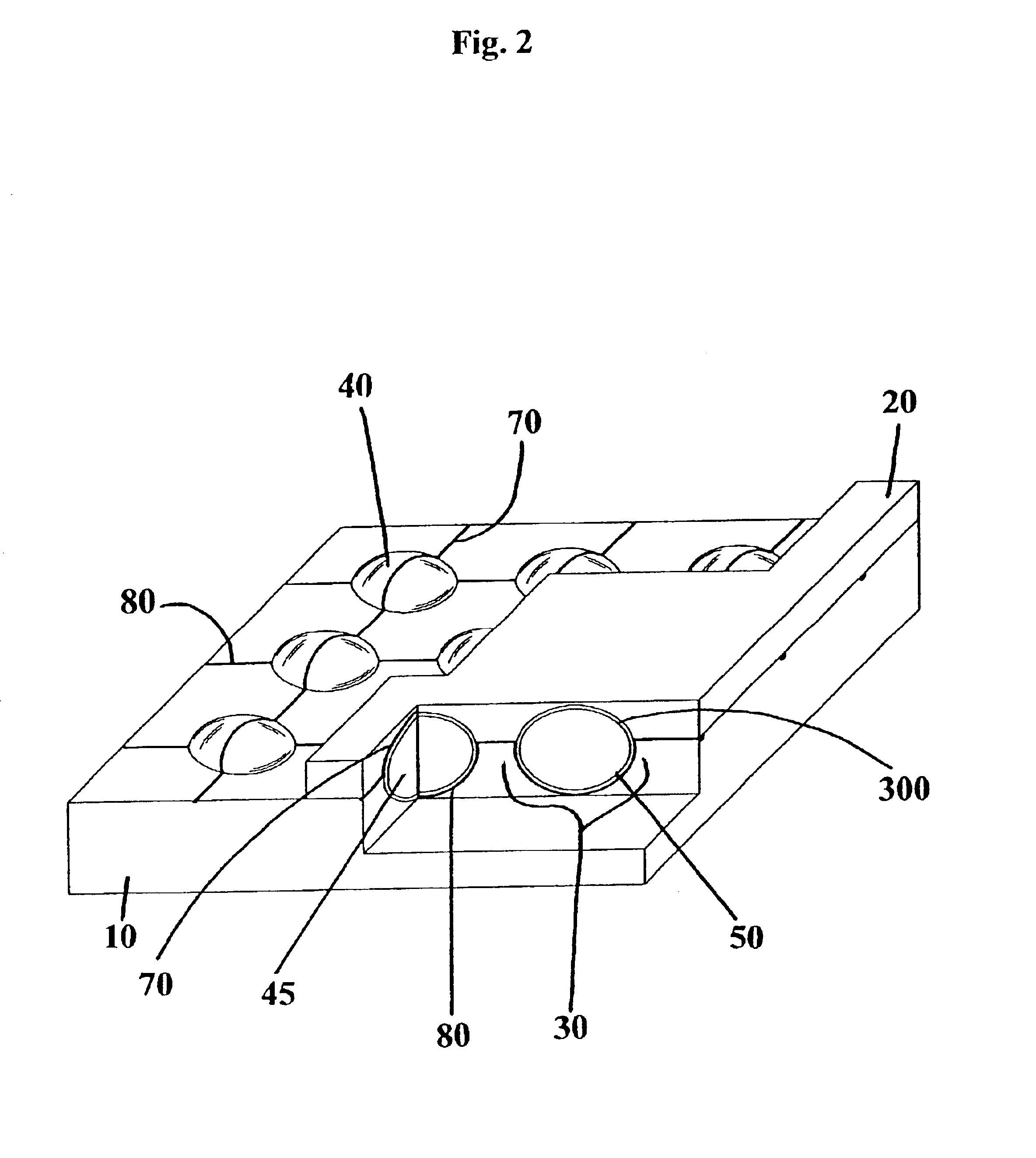
FIGS. 1 and 2 show two embodiments of the present invention wherein a light-emitting panel includes a first substrate 10 and a second substrate 20. The first substrate 10 may be made from silicates, polypropylene, quartz, glass, any polymeric-based material or any material or combination of materials known to one skilled in the art. Similarly, second substrate 20 may be made from silicates, polypropylene, quartz, glass, any polymeric-based material or any material or combination of materials known to one skilled in the art. First substrate 10 and second substrate 20 may both be made from the same material or each of a different material. Additionally, the first and second substrate may be made of a ma...


PUM

PropertyMeasurementUnit
radiating wavelengthsaaaaaaaaaa
diameteraaaaaaaaaa

Abstract

An improved light-emitting panel having a plurality of micro-components sandwiched between two substrates is disclosed. Each micro-component contains a gas or gas-mixture capable of ionization when a sufficiently large voltage is supplied across the micro-component via at least two electrodes. An improved method of manufacturing a light-emitting panel is also disclosed, which uses a web fabrication process to manufacturing light-emitting displays as part of a high-speed, continuous inline process.

Description

1. Field of the InventionThe present invention is related to a light-emitting panel and methods of fabricating the same. The present invention further relates to a web fabrication process for manufacturing a light-emitting panel.2. Description of Related ArtIn a typical plasma display, a gas or mixture of gases is enclosed between orthogonally crossed and spaced conductors. The crossed conductors define a matrix of cross over points, arranged as an array of miniature picture elements (pixels), which provide light. At any given pixel, the orthogonally crossed and spaced conductors function as opposed plates of a capacitor, with the enclosed gas serving as a dielectric. When a sufficiently large voltage is applied, the gas at the pixel breaks down creating free electrons that are drawn to the positive conductor and positively charged gas ions that are drawn to the negatively charged conductor. These free electrons and positively charged gas ions collide with other gas atoms causing an...

Claims


Application Information

Patent Timeline
Patent Type & Authority Patents(United States)
IPC IPC(8): F21V8/00H01J17/49A61N5/06A61L2/10B01J19/12B41MH01J9/02H01J9/24H01J9/395H01J9/48H01J17/16H01J65/04H04N5/66
CPCA61L2/10A61L9/20G02B6/0033G02B6/0036G02B6/0065H01J9/185H01J9/241H01J9/245H01J9/395H01J9/48H01J11/18H01J17/16H01J17/49H01J65/046H01J2217/49264H01J2217/49285H01J9/24
Inventor GEORGE, E. VICTORGREEN, ALBERT M.WYETH, N. CONVERS
Owner LEIDOS
Why Eureka
Try Eureka