

MOS transistor structure and method of fabrication
a technology of mos transistors and mos, which is applied in the direction of semiconductor devices, electrical equipment, radio frequency controlled devices, etc., can solve the problems that the structure and method of fabrication of conventional mos transistors cannot be simply "scaled down" to produce smaller transistors for higher density integration, and the present techniques cannot scale the size of the tip region to support the scaling of the gate length
- Summary
- Abstract
- Description
- Claims
- Application Information
AI Technical Summary
Benefits of technology
Problems solved by technology
Method used
Image

Examples
Embodiment Construction
A novel metal oxide semiconductor (MOS) field effect transistor and its method of fabrication is described. In the following description numerous specific details are set forth such as specific materials, dimensions, and processes etc. in order to provide a thorough understanding of the present invention. It will be obvious, however, to one skilled in the art that the present invention may be practiced without the specific details. In other instances well known semiconductor equipment and processes have not been described in particular detail in order to avoid unnecessarily obscuring the present invention.
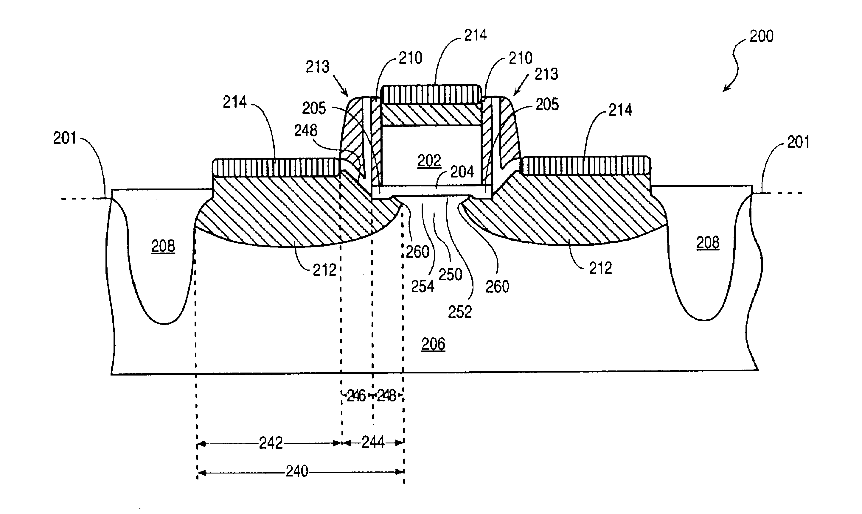
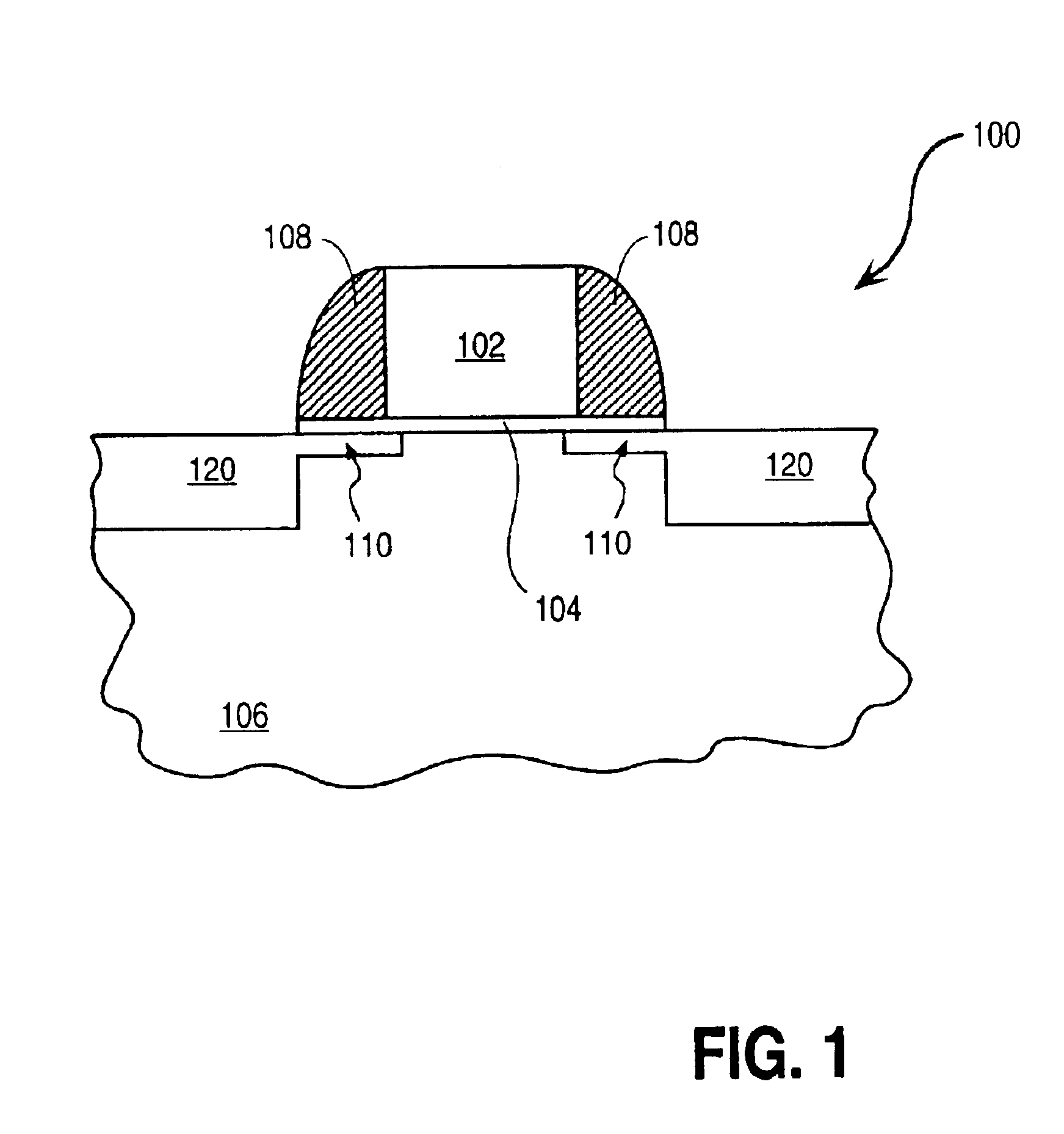
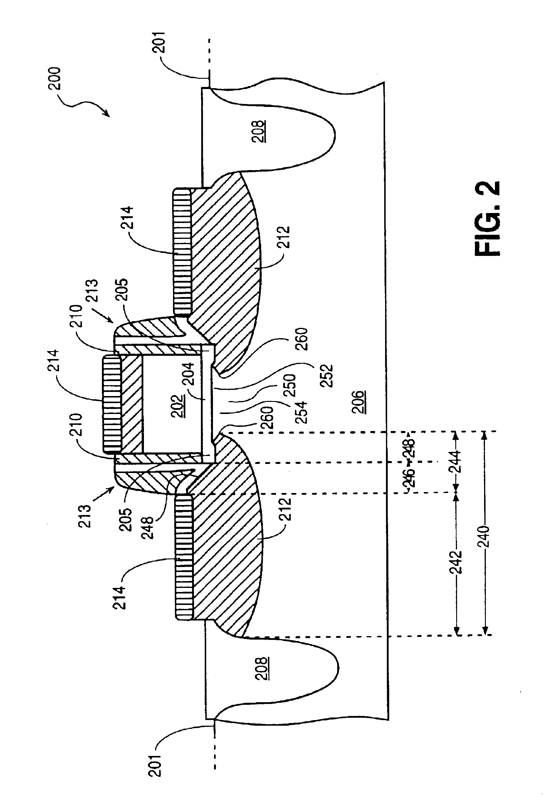
The present invention is a novel MOS transistor structure with improved performance and scalability and its method of fabrication. In one embodiment of the present invention the structure includes inwardly concaved source / drain regions formed with deposited silicon or silicon alloys. The inwardly concaved source / drain regions create a channel region which is larger at the silicon / g...
PUM
| Property | Measurement | Unit |
|---|---|---|
| gate lengths | aaaaa | aaaaa |
| lengths | aaaaa | aaaaa |
| drawn length | aaaaa | aaaaa |
Abstract
Description
Claims
Application Information