Off-chip inductor

a technology of inductor and chip, applied in the field of semiconductor chip fabrication, can solve the problems of increasing the area required for the inductor, affecting the manufacturing process, and requiring additional processing of the wafer during fabrication

Inactive Publication Date: 2004-10-12
SKYWORKS SOLUTIONS INC
View PDF10 Cites 31 Cited by
  • Summary
  • Abstract
  • Description
  • Claims
  • Application Information

AI Technical Summary

Problems solved by technology

However, each of the current approaches has various undesirable side effects associated with it.
However, when designing an inductor into the semiconductor die, the amount of area required for the inductor increases the size of the semiconductor die and additional processing of the wafer during fabrication might also be required.
Both increasing the size of the semiconductor die and additional processing of the wafer increase the cost and also adversely impacts the yield of the semiconductor die.
These additional steps in the assembly process, such as surface mounting of the discrete inductors, increases the overall cost of the assembly, and may also reduce the assembly yield.
Further, surface mounting discrete inductors onto the package substrate increases the overall size of the assembly.
However, once the printed inductor has been defined on the package substrate, the inductance of the printed inductor cannot be altered without redesigning the package substrate.
Although this option allows the inductance of printed inductor to be adjusted to meet a required value, the above option is costly and difficult to implement.
Further, there exists a need in the art for structure and method for fabricating an inductor on the surface of a semiconductor die that is cost effective and does not increase the size of the semiconductor die.

Method used


Image

  • Off-chip inductor
  • Off-chip inductor
  • Off-chip inductor

Examples


Embodiment Construction

The present invention is directed to an off-chip inductor. The following description contains specific information pertaining to various embodiments and implementations of the invention. One skilled in the art will recognize that the present invention may be practiced in a manner different from that specifically discussed in the present application. Moreover, some of the specific details of the invention are not discussed in order not to obscure the invention. The specific details not described in the present application are within the knowledge of a person of ordinary skills in the art.

The drawings in the present application and their accompanying detailed description are directed to merely example embodiments of the invention. To maintain brevity, other embodiments of the invention that use the principles of the present invention are not specifically described in the present application and are not specifically illustrated by the present drawings.

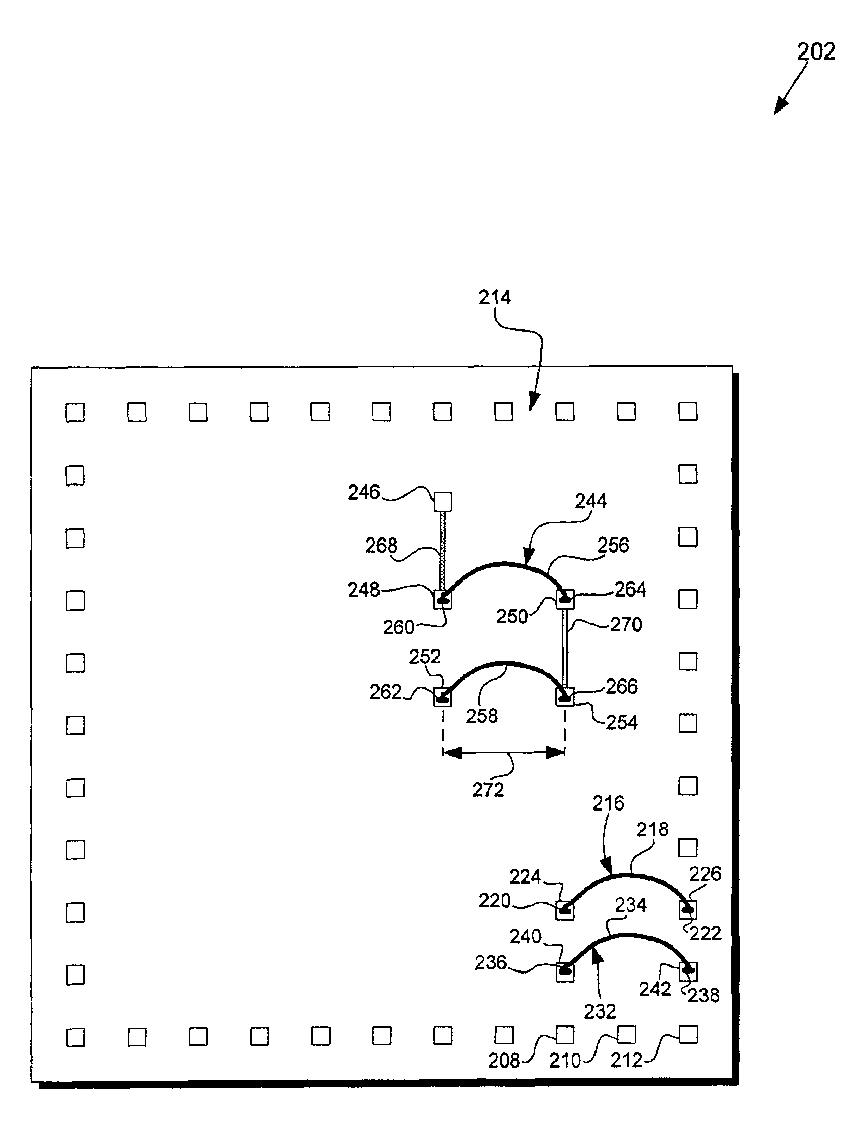
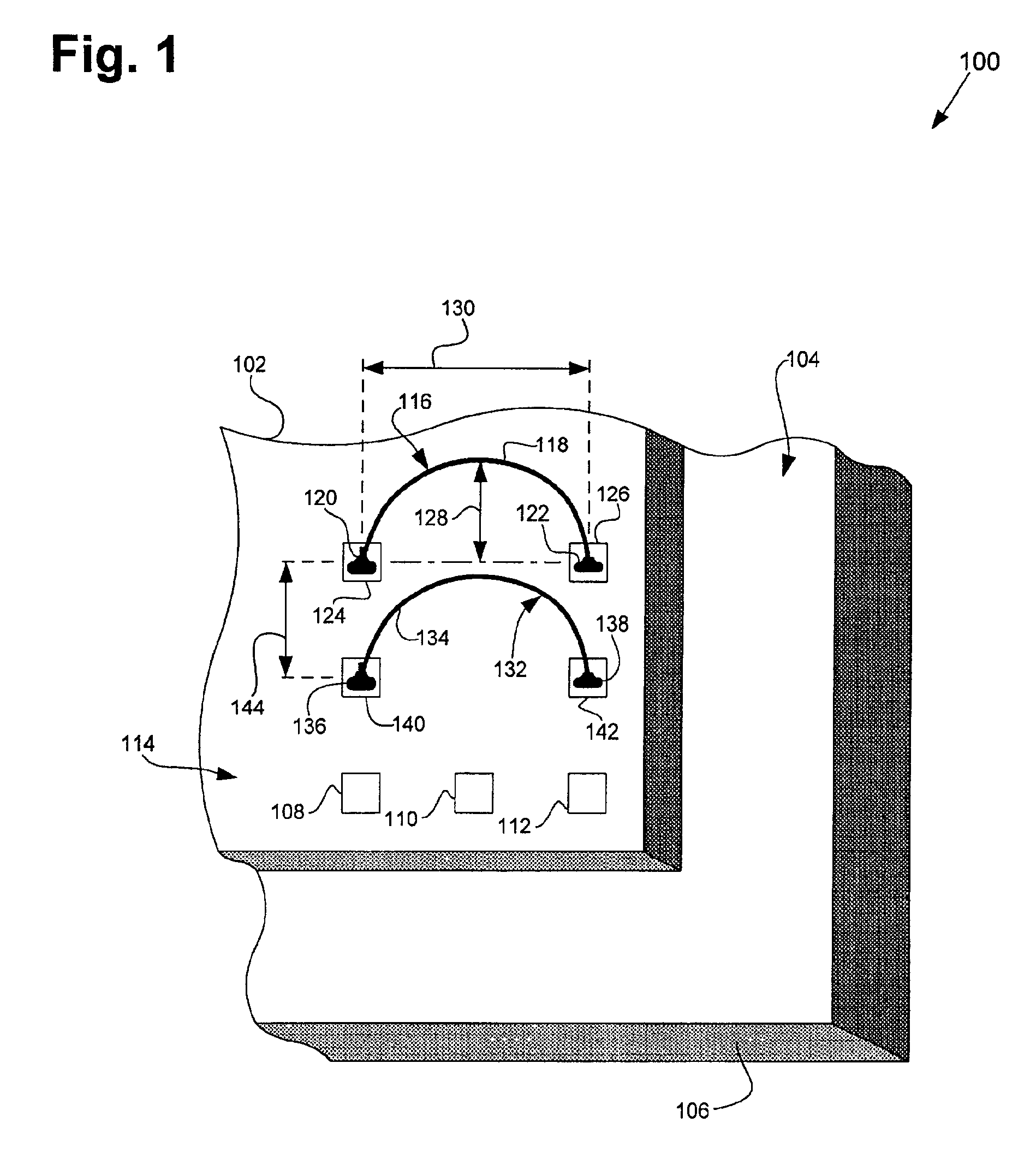
Structure 100 in FIG. 1 illustrate...


PUM

PropertyMeasurementUnit
diameteraaaaaaaaaa
heightaaaaaaaaaa
distanceaaaaaaaaaa

Abstract

According to an embodiment, a semiconductor die has a source bond pad and a destination bond pad attached to a top surface of the semiconductor die. A stud bump is situated on the destination bond pad. A bonding wire is then ball bonded to the source bond pad and thereafter stitch bonded to the stud bump on the destination bond pad. The bonding wire acts as an off-chip inductor or a portion of an off-chip inductor. In one embodiment a number of bonding-wires and on chip conductors are used to form an off-chip inductor. The inductance of the off-chip inductor can be adjusted or fine-tuned by adjusting a loop height of the one or more bonding wires used in the off-chip inductor. The inductance of the invention's off-chip inductor can also be adjusted by increasing or decreasing the number of bonding wires used to form the off-chip inductor.

Description

1. Field of the InventionThe present invention is generally in the field of semiconductor chip fabrication. More specifically, the present invention is in the field of inductors for semiconductor chips.2. Background ArtThe requirement of smaller, more complex, and faster devices operating at high frequencies, such as wireless communications devices and Bluetooth RF transceivers, has also resulted in an increased demand for small size inductors. These small wireless communication devices and Bluetooth RF transceivers contain semiconductor chip packages and semiconductor dies with power and low noise amplifiers that require small size, high quality factor ("Q") inductors for use in the resonance and matching circuits. Various approaches are currently used for adding small size inductors to semiconductor chip packages and semiconductor dies. However, each of the current approaches has various undesirable side effects associated with it.One approach for adding small size inductors invol...

Claims


Application Information

Patent Timeline
Patent Type & Authority Patents(United States)
IPC IPC(8): B23K20/00H01L23/58H01L23/64H01L23/52H01L23/522
CPCB23K20/004B23K20/007H01L23/5227H01L23/645H01L24/48H01L24/85B23K2201/40H01L24/45H01L2223/6611H01L2224/05624H01L2224/05644H01L2224/05647H01L2224/45015H01L2224/45124H01L2224/45144H01L2224/45147H01L2224/48091H01L2224/4813H01L2224/48464H01L2224/48644H01L2224/48647H01L2224/48744H01L2224/48747H01L2224/48824H01L2224/48844H01L2224/78301H01L2224/85205H01L2924/01013H01L2924/01015H01L2924/01029H01L2924/01079H01L2924/19042H01L2924/19104H01L2924/20753H01L2924/30107H01L2924/00014H01L2924/01033H01L2224/48624H01L2224/48847H01L2224/48724H01L2224/78H01L2924/00B23K2101/40H01L2224/05554H01L2924/00015
Inventor MEGAHED, MOHAMED A.COTE, KEVIN J.HASHEMI, HASSAN S.
Owner SKYWORKS SOLUTIONS INC
Why Eureka
Try Eureka