Luminescence crystal particle, luminescence crystal particle composition, display panel and flat-panel display

a technology of luminescence crystal particle and composition, which is applied in the manufacture of electric discharge tubes/lamps, tubes with screens, discharge tubes, etc., can solve the problems of phosphor particles with which electrons collide constantly, difficulty in increasing electron-accelerating voltage to the level of electron-accelerating voltage in cathode ray tubes, and deterioration of the display quality of cold cathode field emission display, etc., to achieve uniform electron-emitting properties.

Inactive Publication Date: 2004-11-16
SONY CORP
View PDF21 Cites 35 Cited by
  • Summary
  • Abstract
  • Description
  • Claims
  • Application Information

AI Technical Summary

Benefits of technology

In the luminescence crystal particle composition of the present invention, water can be used as a dispersing medium. The luminescence crystal particle composition of the present invention may contain polyvinyl alcohol as a dispersing agent or a retaining agent, and ammonium bichromate may be used as a photosensitive polymer. The luminescence crystal particles of the present invention may be surface-treated for improving the dispersing property and adhesion thereof.
In the cold cathode field emission device having the first structure of a crown-type cold cathode field emission device, the material for constituting an electron-emitting portion includes electrically conductive particles and a combination of electrically conductive particles with a binder. The material of the electrically conductive particles includes carbon-containing materials such as graphite; refractory metals such as tungsten (W), niobium (Nb), tantalum (Ta), titanium (Ti), molybdenum (Mo) and chromium (Cr); and transparent electrically conductive materials such as ITO (indium tin oxide). The binder includes glass such as water glass and general purpose resins. Examples of the general purpose resins include thermoplastic resins such as a vinyl chloride resin, a polyolefin resin, a polyamide resin, a cellulose ester resin and a fluorine resin, and thermosetting resins such as an epoxy resin, an acrylic resin and a polyester resin. For improving electron emission efficiency, preferably, the particle size of the electrically conductive particles is sufficiently small as compared with dimensions of the electron-emitting portion. Although not specially limited, the form of the electrically conductive particles is spherical, polyhedral, plate-like, acicular, columnar or amorphous. Preferably, the electrically conductive particles have such a form that exposed portions of the particles form acute projections. Electrically conductive particles having different dimensions and different forms may be used as a mixture.
As a material for constituting an electron-emitting portion, particularly, carbon is preferred. More specifically, diamond is preferred, and above all, amorphous diamond is preferred. When the electron-emitting portion is made of amorphous diamond, an emitted-electron current density necessary for the flat-panel display can be obtained at an electric field intensity of 5.times.10.sup.7 V / m or lower. Further, since amorphous diamond is an electric resister, emitted-electron currents obtained from the electron-emitting portions can be brought into uniform currents, and the fluctuation of brightness can be suppressed when such cold cathode field emission devices are incorporated into a flat-panel display. Further, since the amorphous diamond exhibits remarkably high durability against sputtering by ions of residual gas in the flat-panel display, cold cathode field emission devices having a longer lifetime can be attained.
In the cold cathode field emission device, a resistance layer may be formed between the cathode electrode and the electron-emitting portion. Otherwise, when the surface of the cathode electrode or the edge portion of the cathode electrode corresponds to the electron-emitting region, the cathode electrode may have a three-layered structure constituted of an electrically conductive material layer, a resistance layer and an electron-emitting layer corresponding to the electron-emitting region. The resistance layer can stabilize performances of the cold cathode field emission device and can attain uniform electron-emitting properties. The material for constituting a resistance layer includes carbon-containing materials such as silicon carbide (SiC); SiN; semiconductor materials such as amorphous silicon and the like; and refractory metal oxides such as ruthenium oxide (RuO.sub.2), tantalum oxide and tantalum nitride. The resistance layer can be formed by a sputtering method, a CVD method or a screen-printing method. The resistance value of the resistance layer is approximately 1.times.10.sup.5 to 1.times.10.sup.7 .OMEGA., preferably several M.OMEGA..

Problems solved by technology

In the cold cathode field emission display that is a flat-panel display, the flying distance of electrons is far smaller than the counterpart in a cathode ray tube, so that it is difficult to increase an electron-accelerating voltage to the level of an electron-accelerating voltage in the cathode ray tube.
In the cold cathode field emission display, if the electron-accelerating voltage is too high, spark discharge is liable to take place between the electron-emitting portion in the back panel and the film which functions as an anode electrode in the display panel, and the display quality of the cold cathode field emission display may be impaired to a great extent.
In addition to the above problem, the cold cathode field emission display for which it is required to select the above low electron-accelerating voltage involves characteristic problems from which the cathode ray tube is free.
Therefore, the phosphor particles with which the electrons collide constantly is deteriorated greatly as compared with other phosphor particles, and the phosphor particles are deteriorated faster that the counterpart in the cathode ray tube.
Further, the outermost surface of the phosphor particle suffers various strains during the processes of producing the phosphor particles and producing the display panel and is liable to have lattice defects.
While the cold cathode field emission display is operated, crystal defects are liable to be formed or multiplied newly in the phosphor particle, which is considered to cause the brightness deterioration to proceed faster.
The above-explained deterioration of the phosphor layer or the phosphor particles results in the fluctuation of emitted-light color and luminescence efficiency, the contamination of internal components of the cold cathode field emission display and a consequent decrease in reliability and lifetime characteristics of the cold cathode field emission display.
In this method, however, the phosphor particles that emit light in green are particularly liable to be damaged, and such a phenomenon leads to the generation of a magenta ring.

Method used


Image

  • Luminescence crystal particle, luminescence crystal particle composition, display panel and flat-panel display
  • Luminescence crystal particle, luminescence crystal particle composition, display panel and flat-panel display
  • Luminescence crystal particle, luminescence crystal particle composition, display panel and flat-panel display

Examples


example 2

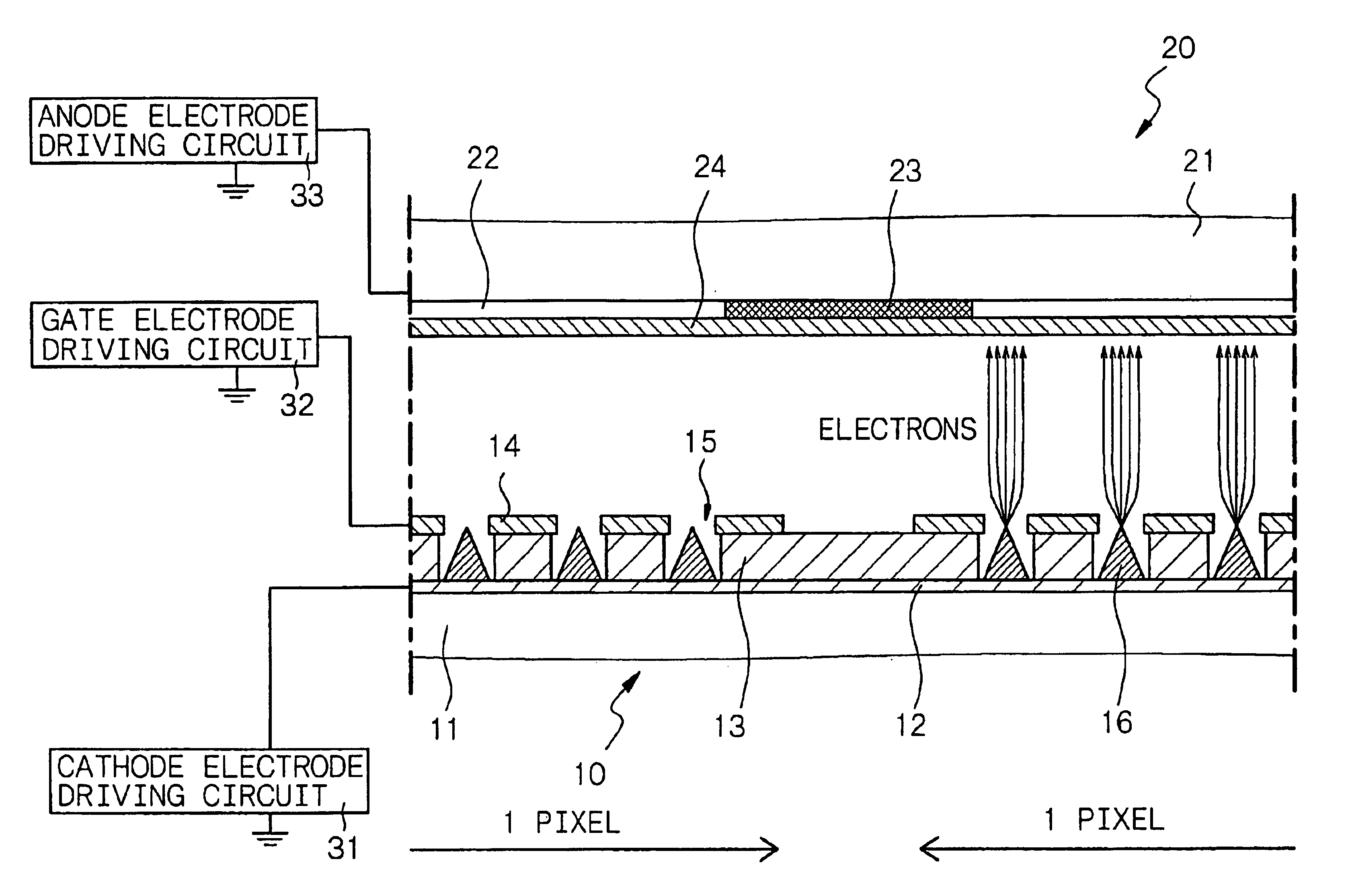
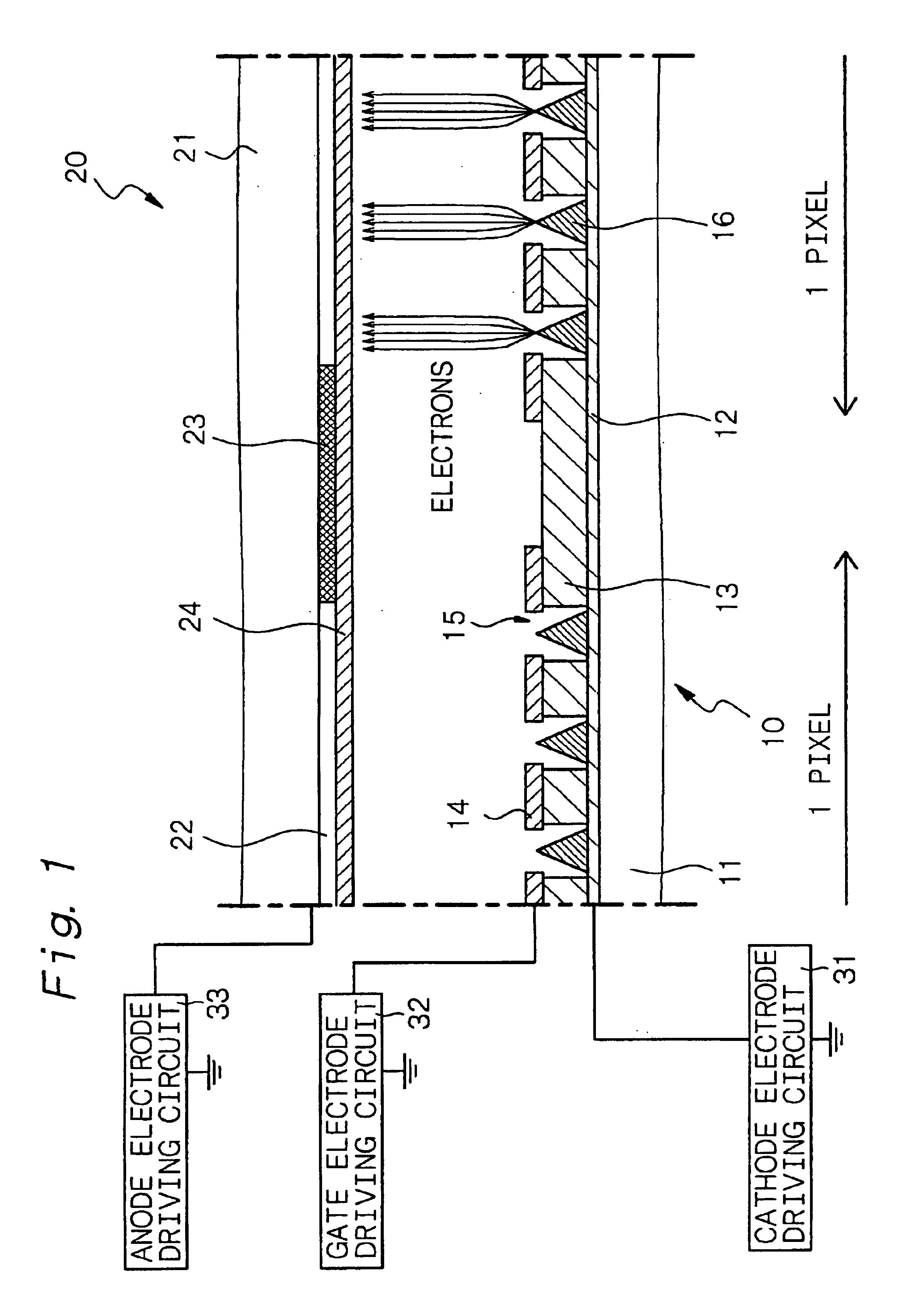
In Examples 2 to 12, various field emission devices will be explained. In Example 2, each electron-emitting region comprises a plurality of crown-type field emission devices. Display panels 20 in Example 2 and Examples 3 to 12 to be described later can be structurally the same as that in Example 1, so that detailed explanations thereof are omitted.

FIG. 9A shows a schematic partial end view of a field emission device having the first structure of a crown-type field emission device, and FIG. 9B shows a partial cut-off schematic perspective view thereof. The crown-type field emission device comprises a cathode electrode 12 formed on a substrate 11; an insulating layer 13 formed on the substrate 11 and the cathode electrode 12; a gate electrode 14 formed on the insulating layer 13; an opening portion 15 penetrating through the gate electrode 14 and the insulating layer 13; and a crown-type electron-emitting portion 16A formed on a portion of the cathode electrode 12 which portion is pos...

example 3

In Example 3, each electron-emitting region is constituted of a plurality of plane-type electron emission devices.

FIG. 10C shows a schematic partial cross-sectional view of a field emission device having the first structure of a plane-type field emission device. The plane-type field emission device comprises a cathode electrode 12 formed on a substrate 11 made, for example, of glass; an insulating layer 13 formed on the substrate 11 and the cathode electrode 12; a gate electrode 14 formed on the insulating layer 13; an opening portion 15 penetrating through the gate electrode 14 and the insulating layer 13; and a flat electron-emitting portion 16B formed on a portion of the cathode electrode 12 which portion is positioned in the bottom portion of the opening portion 15. The electron-emitting portion 16B is formed on the cathode electrode 12 in the form of a stripe extending in the direction perpendicular to the paper surface of FIG. 10C. Further, the gate electrode 14 extends leftwa...

example 4

FIG. 11C shows a schematic partial cross-sectional view of a variant of the field emission device having the first structure of the plane-type field emission device. The plane-type field emission device shown in FIG. 11C differs from the plane-type field emission device shown in FIG. 10C in the structure of the electron-emitting portion 16B to some extent. The method for producing such a field emission device will be explained below with reference to FIGS. 11A, 11B and 11C showing schematic partial cross-sectional views of the substrate, etc.

[Step-400]

First, the electrically conductive material layer for a cathode electrode is formed on the substrate 11. Specifically, a resist material layer (not shown) is formed on the entire surface of the substrate 11, and then the resist material layer is removed from a portion where the cathode electrode is to be formed. Then, the electrically conductive material layer made of chromium (Cr) for a cathode electrode is formed on the entire surfac...


PUM

PropertyMeasurementUnit
energyaaaaaaaaaa
energyaaaaaaaaaa
wavelengthaaaaaaaaaa

Abstract

A luminescence crystal particle which emits light upon irradiation with an energy beam and which has a crystal defect density of 5x10<7 >defects / cm<2 >or less in a region located from the surface of the luminescence crystal particle to a portion as deep as the energy beam reaches.

Description

BACKGROUND OF THE INVENTION AND RELATED ART STATEMENTThe present invention relates to a luminescence crystal particle which emits light upon irradiation with an energy beam, a luminescence crystal particle composition, a display panel constituted of such luminescence crystal particles and a flat-panel display having such a display panel.As an image display device that can be substituted for a currently mainstream cathode ray tube (CRT), flat-screen (flat-panel) displays are studied in various ways. Such fat-panel displays include a liquid crystal display (LCD), an electroluminescence display (ELD) and a plasma display (PDP). There has been also proposed a cold cathode field emission display capable of emitting electrons into a vacuum from a solid without relying on thermal excitation, a so-called field emission display (FED), and it attracts attention from the viewpoint of the brightness of a display screen and low power consumption.FIG. 1 shows a typical constitution of the cold ca...

Claims


Application Information

Patent Timeline
Patent Type & Authority Patents(United States)
IPC IPC(8): C09K11/00H01J31/12C09K11/08C09K11/56C09K11/84H01J1/30H01J1/63H01J9/227H01J11/22H01J11/34H01J11/42H01J29/20
CPCC09K11/642H01J31/123C09K11/7789H01J1/30H01J9/227
Inventor KAJIWARA, KAZUO
Owner SONY CORP
Why Eureka
Try Eureka