Structure having embedded flush circuitry features and method of fabricating

Inactive Publication Date: 2005-01-11
GLOBALFOUNDRIES US INC
View PDF15 Cites 6 Cited by
  • Summary
  • Abstract
  • Description
  • Claims
  • Application Information

AI Technical Summary

Benefits of technology

The present invention provides for obtaining a structure having dense embedded flush circuitry features. The present invention makes it possible to create circuitry features that are much more dense

Problems solved by technology

For instance, the complexity, compactness and electrical performance requirements of printed boards have significantly increased over the last several years.
Smooth copper layers do not adequately bond without an auxiliary bonding agent.
Great difficulties exist in adequately etching dendrites especially when dealing with small spaces.
Moreover, along with the concern created by dendrites, the width of the lines (e.g. about 0.5 mils wide), and photolithographic issues (e.g. resolution of fine features, 0.7 mil wire with 1.1

Method used


Image

  • Structure having embedded flush circuitry features and method of fabricating
  • Structure having embedded flush circuitry features and method of fabricating

Examples


Example

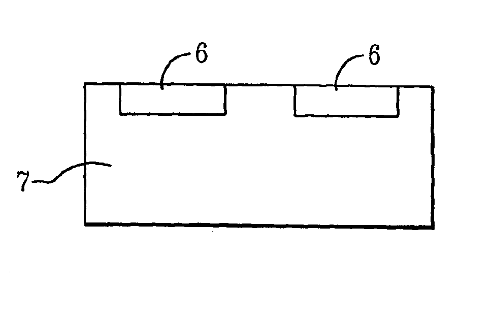
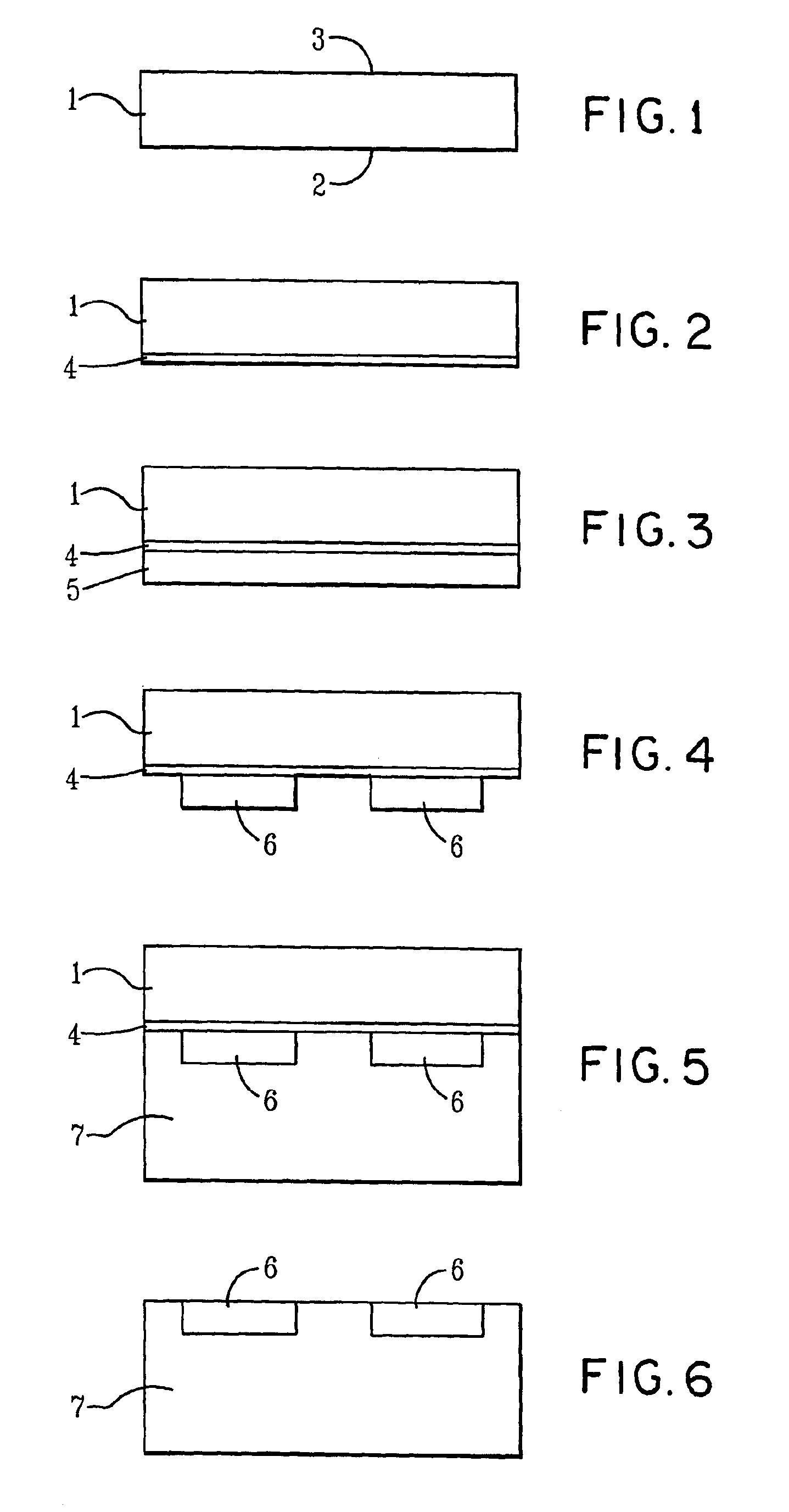
As shown in FIG. 1, the structure of the present invention having embedded flush or coplanar circuitry features can be produced by employing a sacrificial carrier film 1 having a front side 2 and a back side 3. Typical sacrificial films include polyimides such as Kapton and Upilex. The sacrificial films are typically about 20 to about 250 microns thick, and more typically about 50 to about 100 microns thick.

The carrier is preferably smooth thereby eliminating metallic dendrites in the subsequently to be provided metal layer.

Next a relatively thin seed layer of a conductive metal 4 is deposited onto the front side of the sacrificial carrier film 1, as illustrated in FIG. 2. Typical metals include copper and chromium with copper being preferred. The seed layer is typically about 500 to about 2000 angstroms thick, a particular example being about 1000 angstroms. The seed layer can be deposited by electroless plating.

A conductive thin film 5 such as copper is then plated onto the seed l...


PUM

PropertyMeasurementUnit
Lengthaaaaaaaaaa
Lengthaaaaaaaaaa
Dielectric polarization enthalpyaaaaaaaaaa

Abstract

Embedded flush circuitry features are provided by depositing a conductive seed layer on the front side of a sacrificial carrier; plating a layer of conductive metal onto the seed layer and personalizing circuitry features. The front side of the carrier film is embedded into a dielectric material and the sacrificial carrier film is removed.

Description

FIELD OF THE INVENTIONThe present invention relates to providing a structure having circuitry features and in particular to embedded flush circuitry features. The present invention is especially advantageous for fabricating buried interconnection levels that are in close proximity to one another in a printed circuit board structure.BACKGROUND OF THE INVENTIONPrinted circuit boards find a wide variety of uses in the electronics industry with the demand for high performance, printed wiring, or circuit boards for various applications steadily increasing. For instance, the complexity, compactness and electrical performance requirements of printed boards have significantly increased over the last several years.The demands on printed circuit boards require high density packaging, fine interconnection, multilayer formation and the need to form a plurality of interconnections in a small space.Currently, printed circuit board interconnection levels are built on top of a dielectric thin film ...

Claims


Application Information

Patent Timeline
IPC IPC(8): H05K3/20
CPCH05K3/20Y10T29/49156Y10T428/24917Y10S428/901
Inventor EDWARDS, ROBERT DOUGLASKNIGHT, JEFFREY ALANMORING, ALLEN FREDERICKWILSON, JAMES W.
Owner GLOBALFOUNDRIES US INC
Why Eureka
Try Eureka