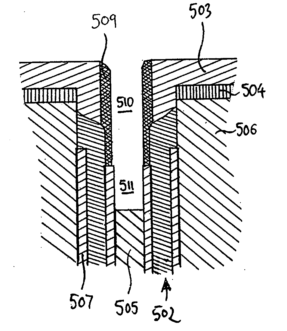
[0011] The isolation element, comprising a broader upper part and a narrower lower part, achieves a higher overall
aspect ratio compared to state of the art isolation elements. While penetrating deep enough into the substrate to suppress vertical parasitic currents, the isolation element provides also suppression of horizontal parasitic currents and is narrow enough for the electronic elements to be arranged closer to each other. Since a higher
aspect ratio of the isolation element translates to a smaller width—keeping constant the height—the electronic elements can be arranged in a denser configuration and hence more electronic elements may be integrated into the circuit. This substantially increases the overall performance of the integrated circuit. The two-part configuration of the isolation element achieves said enhanced aspect ratio while allowing for an efficient and reliable fabrication of the isolation element by established manufacturing processes.
[0013] The inventive integrated memory device may include an increased number of memory cells, providing an enhanced overall performance of the integrated memory device. Since the
shallow trench isolation elements, comprising a broader upper part and a narrower lower part, may be manufactured with an enhanced aspect ratio, the memory cells can be arranged closer to each other. The enhanced aspect ratio still provides a height of the
shallow trench isolation elements for sufficient vertical electric isolation, while being narrower for a denser packing of the memory cells. In this way, undesired both
horizontal and vertical parasitic currents and interference are still suppressed.
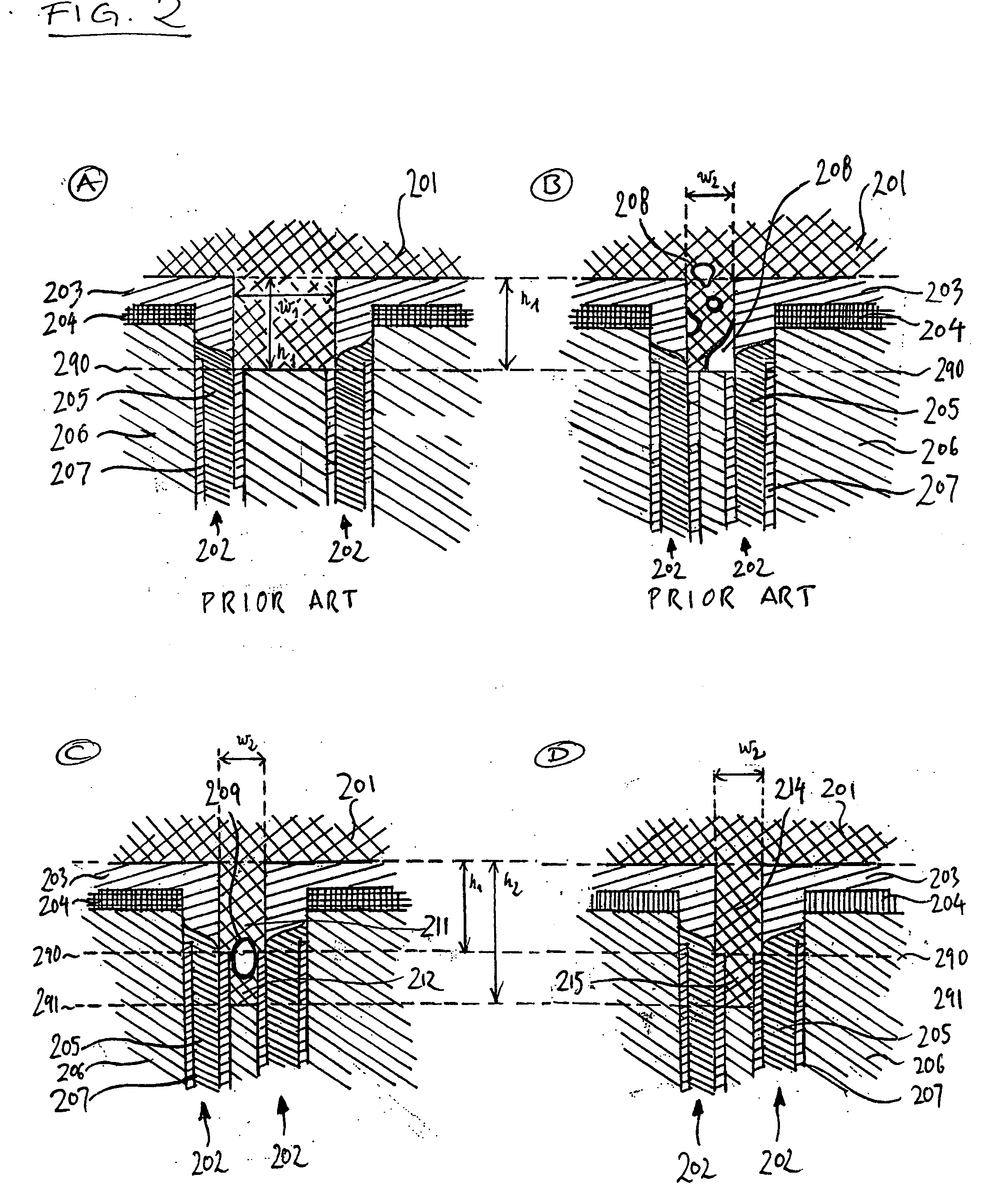
[0018] According to another embodiment of the present invention, the height of the upper part of the isolation elements ranges from 100 to 300 nm. The height of the lower part of the isolation elements ranges, preferably, from 50 to 200 nm. An isolation element, comprising an upper broader part and a lower narrower part, with the heights in the ranges provides sufficient electric isolation and hence a sufficient suppression of vertical parasitic currents and interference.
[0020] Hence, an aspect ratio translates a given height to a width of the isolation element. For an enhanced aspect ratio, the width can be reduced while keeping a given height. In this way, the inventive isolation elements provide a sufficient height for suppressing vertical parasitic currents and interference in combination with a reduced width and hence allow for a denser packing of electronic elements. Parasitic currents and interference is still suppressed, and the overall performance of the integrated circuit is enhanced.
[0021] According to another embodiment, the isolation element comprises a
high density plasma oxide (HDP
oxide). Said HDP oxide is preferably deposited and processed by established manufacturing processes for highly integrated circuits and devices. Furthermore, HDP oxide provides sufficient electric isolation of adjacent electronic elements.
[0024] The present invention provides a void for electric isolation within the isolation element, preferably, situated mainly in the lower part of the isolation element. Although a filling process may not provide complete filling, the invention places a void at the lower part of an isolation element, hence providing both
electrical isolation and an undisturbed top surface of the isolation element for further standard
processing of the integrated circuit. Hence, failure-free manufacturing of the integrated circuit and memory device with standard established process techniques is provided, and an enhanced device performance of the ready integrated circuit is achieved.

