Structure having flush circuit features and method of making

a technology of flush circuit and circuit structure, applied in the direction of printed circuit manufacturing, printed circuit non-printed electric components association, transportation and packaging, etc., can solve the problems of large difficulty in adequately etching dendrites, complex and compact requirements of printed boards, and large increase in compactness and electrical performance requirements of printed boards

Inactive Publication Date: 2005-01-27
IBM CORP
View PDF18 Cites 0 Cited by
  • Summary
  • Abstract
  • Description
  • Claims
  • Application Information

AI Technical Summary

Benefits of technology

[0008] The present invention provides for obtaining a structure having dense embedded flush circuitry features. The present invention makes it possible to create circuitry features that are much more densely configured than those fabricated using current methods. This is made possible since the final structure is a circuitry feature have dielectric regions and conductive features that are coplanar.

Problems solved by technology

For instance, the complexity, compactness and electrical performance requirements of printed boards have significantly increased over the last several years.
Smooth copper layers do not adequately bond without an auxiliary bonding agent.
Great difficulties exist in adequately etching dendrites especially when dealing with small spaces.
Additionally, this subtractive etch approach results in unprotected circuitry features referred to as “skyscrapers” that extend above an underlying plane of dielectric barrier material.
The “skyscraper” structure causes a problem of bridging or shortening between lines especially where there exist closely spaced fingers due to seed.

Method used


Image

  • Structure having flush circuit features and method of making
  • Structure having flush circuit features and method of making
  • Structure having flush circuit features and method of making

Examples


Embodiment Construction

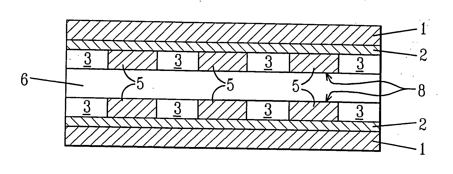
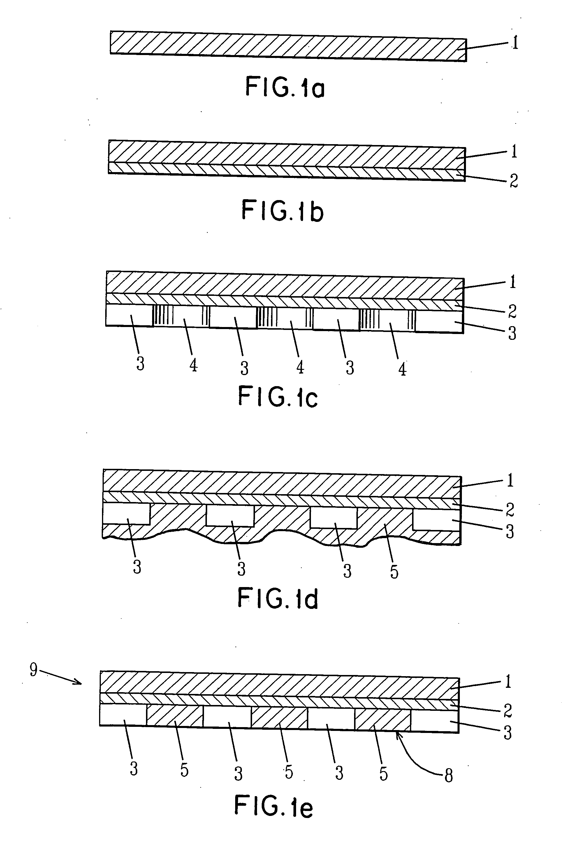
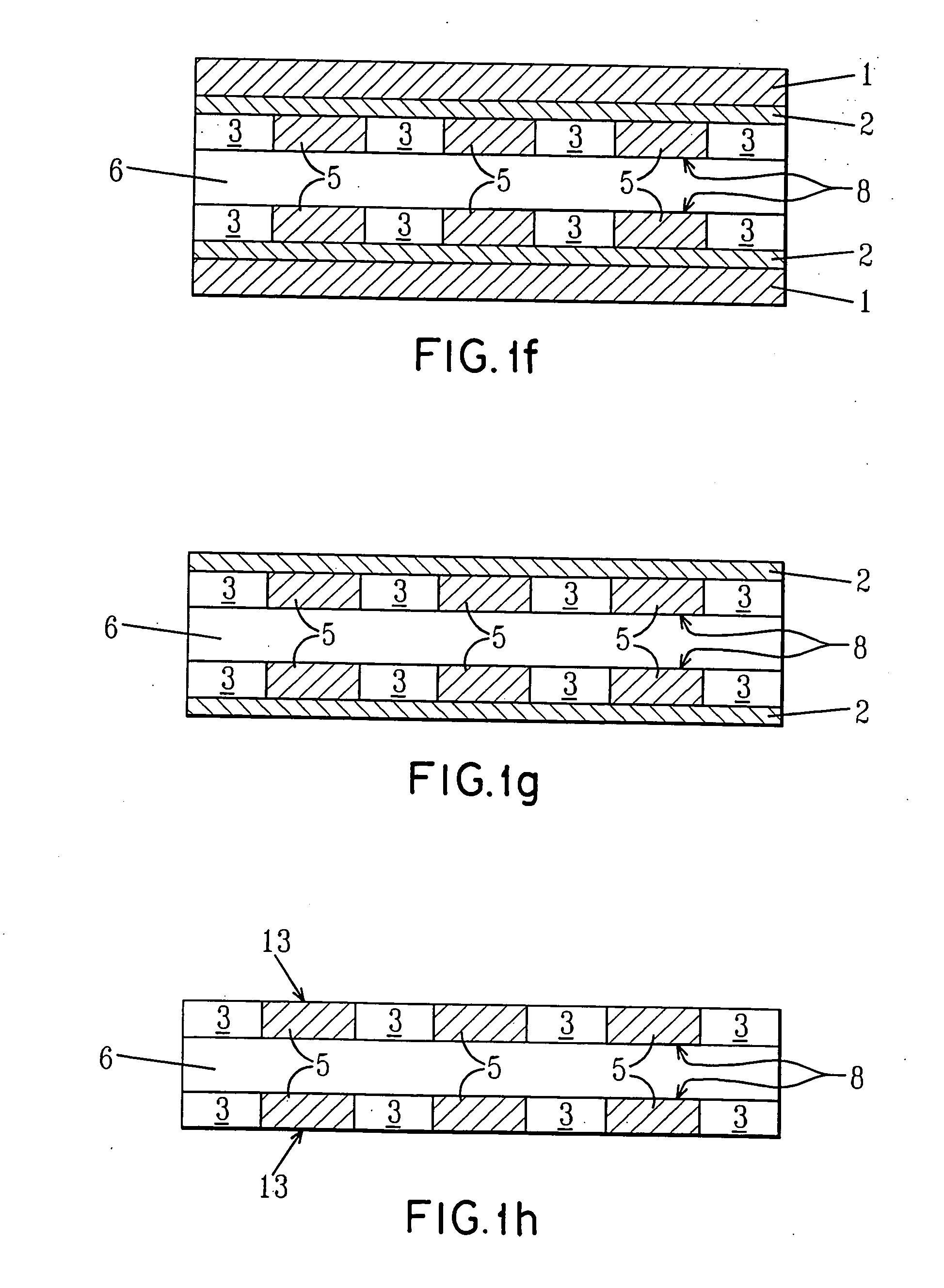
[0024] In order to facilitate an understanding of the present invention, reference will be made to the figures where the same numeral in different figures refers to the same member.

[0025]FIG. 1a illustrates a carrier foil 1 typically a copper foil. The carrier foil 1 can include a top smooth metallized surface and a bottom rough or dendrite surface.

[0026] The foil is typically 9 to about 72 microns thick and more typically about 12 to about 18 microns thick. Typically, suitable copper foils include 0.5 oz and 1 oz foils.

[0027]FIG. 1b illustrates blanket coating an electrically conductive layer 2 onto the top smooth metallized surface of carrier foil 1. An example of a suitable electrically conductive layer 2 is chromium which can be deposited by sputtering or evaporation. The layer 2 is typically about 500 to about 5000 angstroms thick and more typically about 800 to about 1500 angstroms thick.

[0028]FIG. 1c illustrates coating the electrically conductive layer 2 with a dielectri...


PUM

PropertyMeasurementUnit
thicknessaaaaaaaaaa
thicknessaaaaaaaaaa
thicknessaaaaaaaaaa

Abstract

Embedded flush circuitry features are provided by providing a carrier foil having an electrically conductive layer therein and coating the electrically conductive layer with a dielectric material. Circuitry features are formed in the dielectric material and conductive metal is plated to fill the circuitry features.

Description

FIELD OF THE INVENTION [0001] The present invention relates to providing a protected, high density circuitry structure and method of fabrication. [0002] The present invention provides a fine dimensioned planar circuitry structure and method which results in a smooth, protected high density circuitry pattern. The present invention is especially advantageous for fabricating buried connection levels that are in close proximity to one another in a printed circuit board structure and also advantageous for enabling clear spacer and finer features for gold wire band. BACKGROUND OF THE INVENTION [0003] Printed circuit boards find a wide variety of uses in the electronics industry with the demand for high performance, printed wiring, or circuit boards for various applications steadily increasing. For instance, the complexity, compactness and electrical performance requirements of printed boards have significantly increased over the last several years. [0004] The demands on printed circuit bo...

Claims


Application Information

Patent Timeline
Patent Type & Authority Applications(United States)
IPC IPC(8): H05K1/11C25D7/12H05K1/02H05K1/18H05K3/18H05K3/20H05K3/22H05K3/46
CPCH05K3/205C25D7/123Y10T428/12569Y10T428/12361Y10T428/12438H01L2224/32245H01L2224/45144H01L2224/48091H01L2224/48227H01L2224/73265H01L2924/00014
Inventor CLOTHIER, RONALDKNIGHT, JEFFREY ALANSEBESTA, ROBERT DAVID
Owner IBM CORP
Why Eureka
Try Eureka