Leadframe for die stacking applications and related die stacking concepts

a technology of die stacking and die splicing, applied in the direction of electrical equipment, semiconductor devices, semiconductor/solid-state device details, etc., can solve the problems of lead wire damage, lead wire bleeding, and potential for a lower, and achieve the effect of high volume and high reliability

Inactive Publication Date: 2005-01-11
STATS CHIPPAC LTD
View PDF12 Cites 37 Cited by
  • Summary
  • Abstract
  • Description
  • Claims
  • Application Information

AI Technical Summary

Benefits of technology

Additional objects of one or more embodiments of the present invention is to provide electrically isolated stacked die leadframe design packages: (a) having higher reliability; (b) providing more ways of die stacking such as one down-set, two down-sets and up-set combination; and (c) manufacturability in high volume and methods of forming same.

Problems solved by technology

However, several problems exist when using current practice methods / electrical isolation techniques such as: potential for resin bleeding (contamination of the bond pad near the bottom encapsulant material layer) and contamination of wire bond pads; potential for damage of the lead wires of the lower die during wirebonding of the upper die and during subsequent handling; potential for a lower moisture sensitive level (MSL) because of the larger die attachment interface areas for both the lower and upper dies; a third element is required to create a Z-axis spacing between the two stacked dies by using either a film or a silicon / ceramic spacer; and a leadframe having a large die pad down-set value is needed which may not be manufacturable in high volume.
MSL level 2 components have about a one year shelf life and MSL level 3 components only have a one week self life before moisture contamination would render the components unreliable / unusable.
Moisture can cause delamination or voids, usually at the chip / die pad interface.

Method used


Image

  • Leadframe for die stacking applications and related die stacking concepts
  • Leadframe for die stacking applications and related die stacking concepts
  • Leadframe for die stacking applications and related die stacking concepts

Examples


seventh embodiment

Alternatively, in the seventh embodiment, and as shown in FIGS. 12 and 13, the inventors have discovered a semiconductor package for packaging stacked dies / chips that consists of discrete outer die pads affixed to the tie bars and a center pad supported by tie bars. In this alternative, the outer ring shaped die pad is not needed.

It is noted that the inner die pad can be of any shape as long as it is within the area of die encircled by the bond pads.

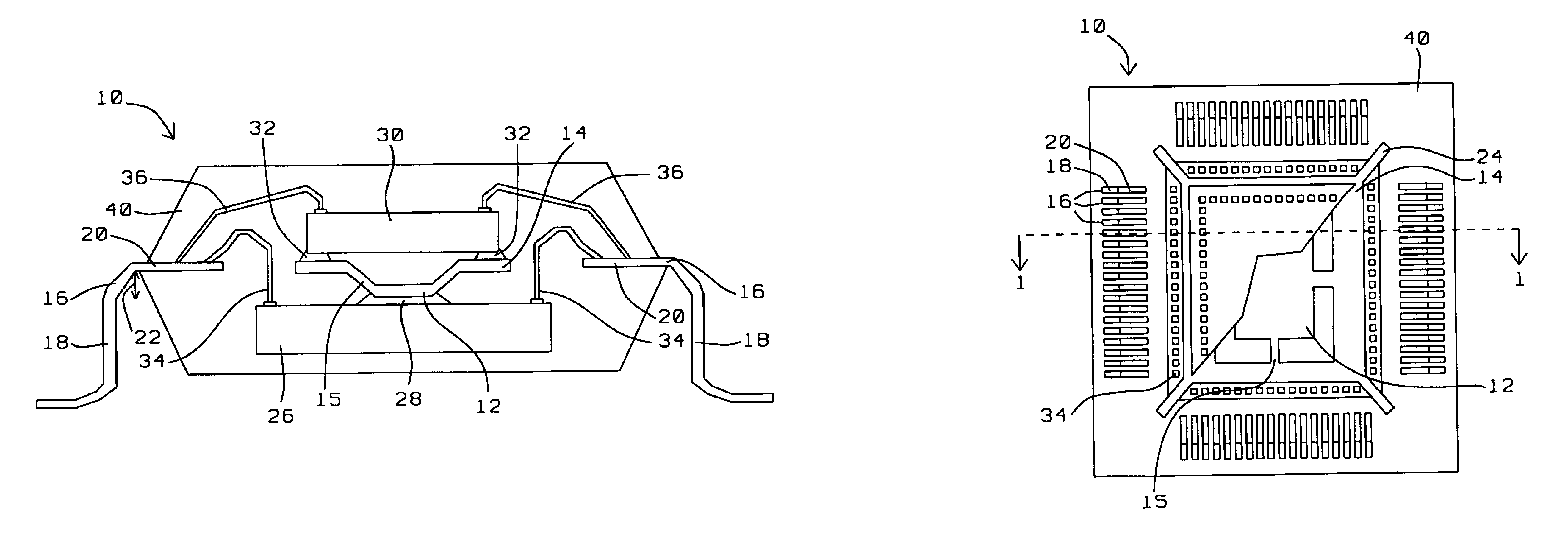
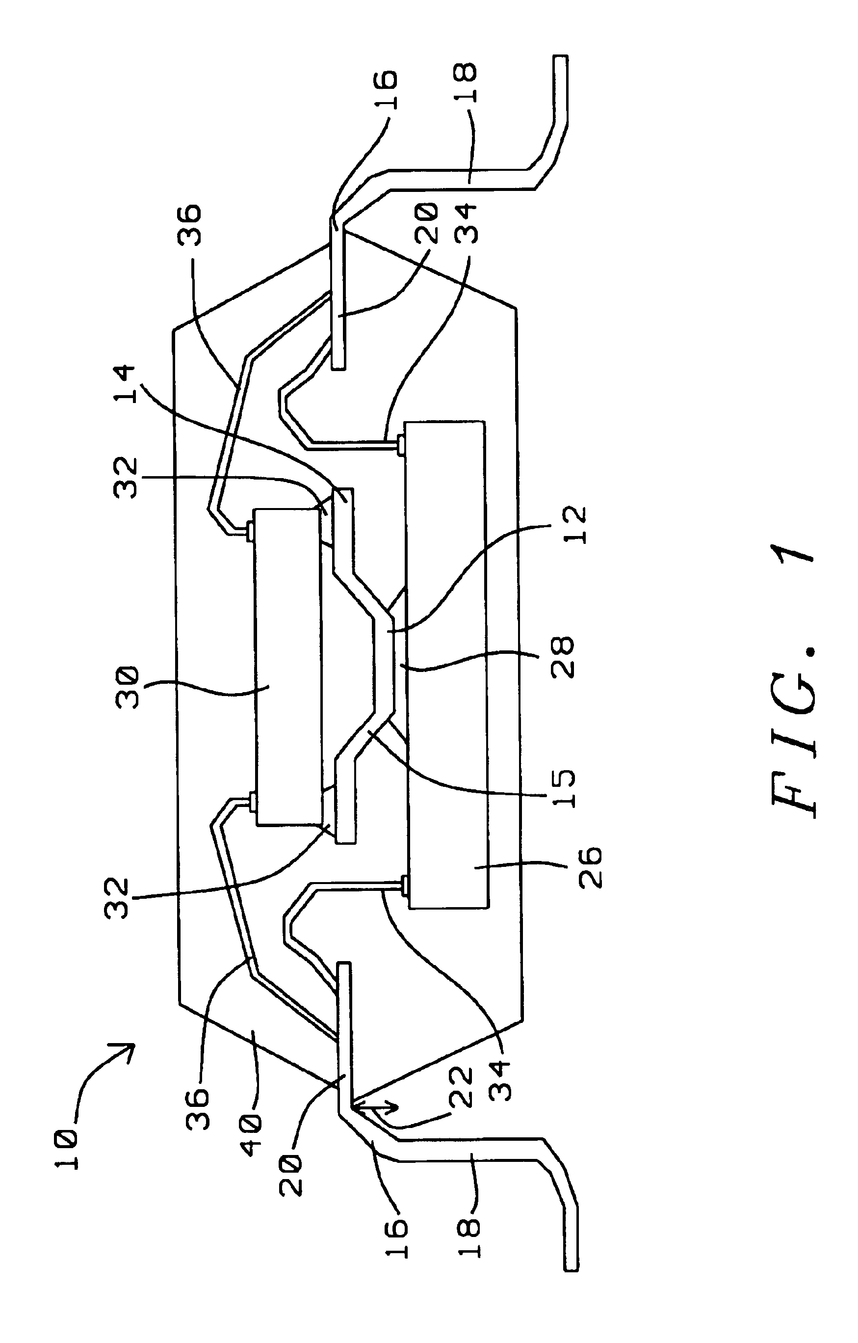
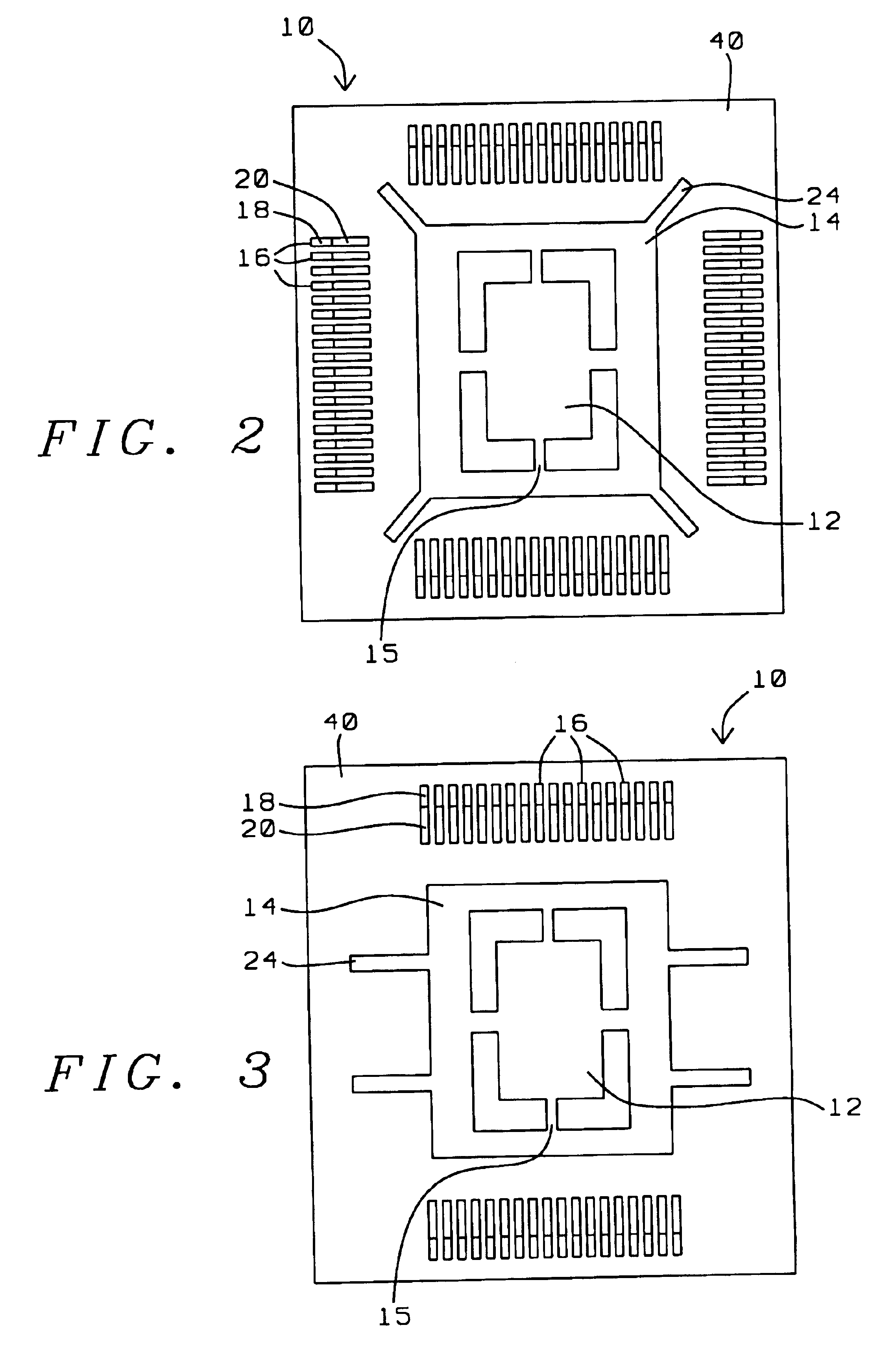
First Embodiment—Single Down-Set of the Inner / Center Die Pad 12; FIGS. 1 to 4

As shown in FIGS. 1 to 4, the first embodiment of the present invention illustrates a package 10 having a leadframe design where there is a single down-set of only the inner / center die pad 12 in relation to the inner portions 20 of lead fingers 16.

Lead fingers 16 include an outer portion 18 exterior of package 10, and an inner portion 20 within package 10.

Inner / center die pad 12 is spaced downwardly (down-set) from inner portions 20 of lead fingers 16 as at 22 f...


PUM


Abstract

A leadframe design (and method of forming the leadframe design), comprising: an inner die pad structure lying in a first plane; and an outer die pad structure supported by outer tie bars and connected to the inner die pad by inner tie bars. The outer die pad structure lying in a second plane spaced apart from the inner die pad structure first plane. An outer package surrounds at least the inner die pad structure and the inner tie bars. The outer die pad structure being supported by the outer tie bars. The outer package having outer walls. Lead fingers extend through the outer package outer walls and include respective inner portions extending into the outer package proximate the inner and outer die pad structures. The inner portions of the lead fingers lie in a third plane, wherein at least one of the inner die pad structure first plane and the outer die pad structure second plane lie outside of the lead finger inner portions third plane and wherein a first chip is affixed to the inner die pad structure and a second chip is affixed to the outer die pad structure.

Description

BACKGROUND OF THE INVENTIONCurrent practice involves electrical isolation of the two stacked dies from each other and the leadframe using an electrically insulating die attach material. However, several problems exist when using current practice methods / electrical isolation techniques such as: potential for resin bleeding (contamination of the bond pad near the bottom encapsulant material layer) and contamination of wire bond pads; potential for damage of the lead wires of the lower die during wirebonding of the upper die and during subsequent handling; potential for a lower moisture sensitive level (MSL) because of the larger die attachment interface areas for both the lower and upper dies; a third element is required to create a Z-axis spacing between the two stacked dies by using either a film or a silicon / ceramic spacer; and a leadframe having a large die pad down-set value is needed which may not be manufacturable in high volume.The moisture sensitive level (MSL) is an importan...

Claims


Application Information

Patent Timeline
Patent Type & Authority Patents(United States)
IPC IPC(8): H01L23/495H01L23/48
CPCH01L23/49503H01L24/32H01L23/49575H01L24/48H01L2224/32014H01L2224/32057H01L2224/32245H01L2224/48091H01L2224/48095H01L2224/48247H01L2224/48472H01L2224/73215H01L2224/73265H01L2224/83385H01L2924/01005H01L2924/01013H01L2924/01075H01L2924/01082H01L2924/14H01L2924/01033H01L2924/01006H01L2924/00014H01L2924/00H01L2924/181H01L2924/12042H01L2224/05554H01L2224/05599H01L2224/45099H01L2224/85399H01L2224/4826H01L2924/00012H01L2224/45015H01L2924/207
Inventor SHIM, IL KWONRAMAKRISHNA, KAMBHAMPATICHOW, SENG GUAN
Owner STATS CHIPPAC LTD
Why Eureka
Try Eureka