Optical element deformation system

a technology of optical elements and deformation systems, applied in the field of optical element deformation systems, can solve problems such as image errors and deformation of optical elements

Inactive Publication Date: 2005-01-18
CARL ZEISS SMT GMBH
View PDF19 Cites 36 Cited by
  • Summary
  • Abstract
  • Description
  • Claims
  • Application Information

AI Technical Summary

Benefits of technology

According to the invention, this object is achieved by means of an optical element deformation system in an purpose of eliminating image errors wherein an optical element bears piezoelectric elements being applied as actuators in the form of thin plates, films or layers to surfaces of the optical element, whereby forces and / or moments are being exerted on the optical element for deformation in conjunction with a servo loop having at least one sensor, and by controlled activation of the piezoelectric elements as actuators.
In an advantageous refinement of the invention, it can also be provided that, to damp vibrations, all the piezoelectric elements are configured as sensors in the quiescent state or in a phase of slight excitation of vibrations. Disturbances which occur are then packed up by all the piezoelectric elements, and all, or else only specific piezoelectric elements can then subsequently be activated as actuators by appropriate control action. This refinement has the advantage that it is not necessary to identify specific piezoelectric elements as sensors or as actuators. All that need be provided is an appropriate regulating or control device.

Problems solved by technology

One of the main causes of image errors in this case is deformations of the optical elements.
Weight forces on optical elements can also lead to deformations and thus to image errors.

Method used


Image

  • Optical element deformation system
  • Optical element deformation system
  • Optical element deformation system

Examples


Embodiment Construction

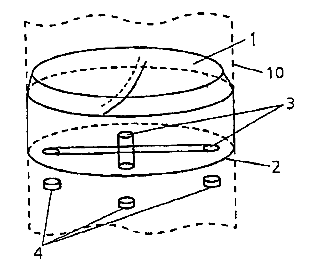
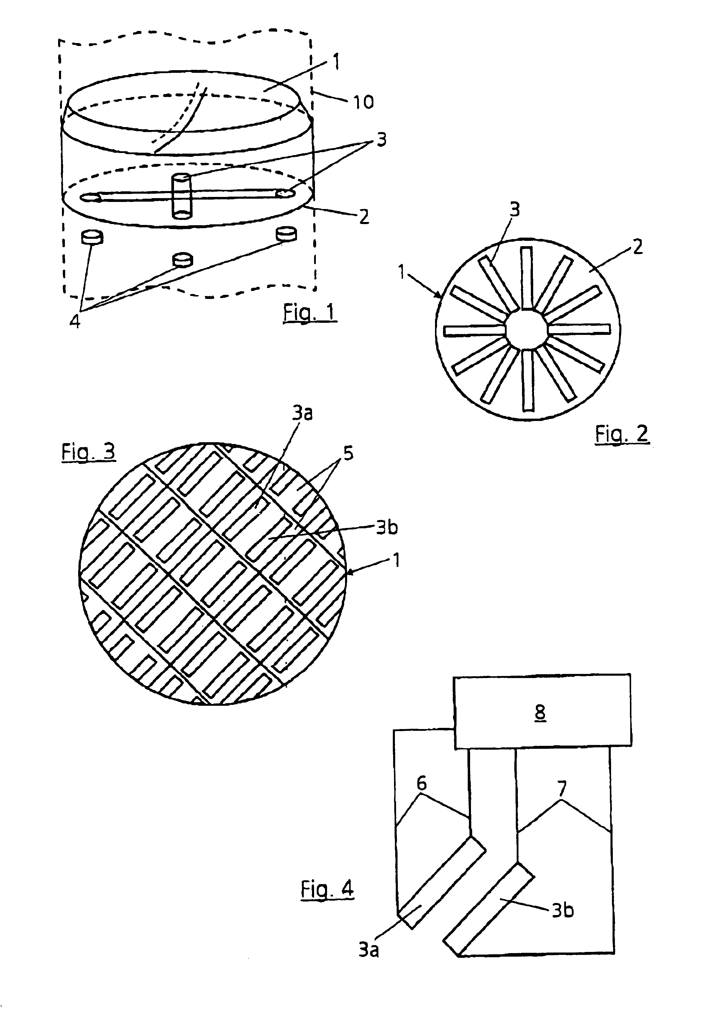
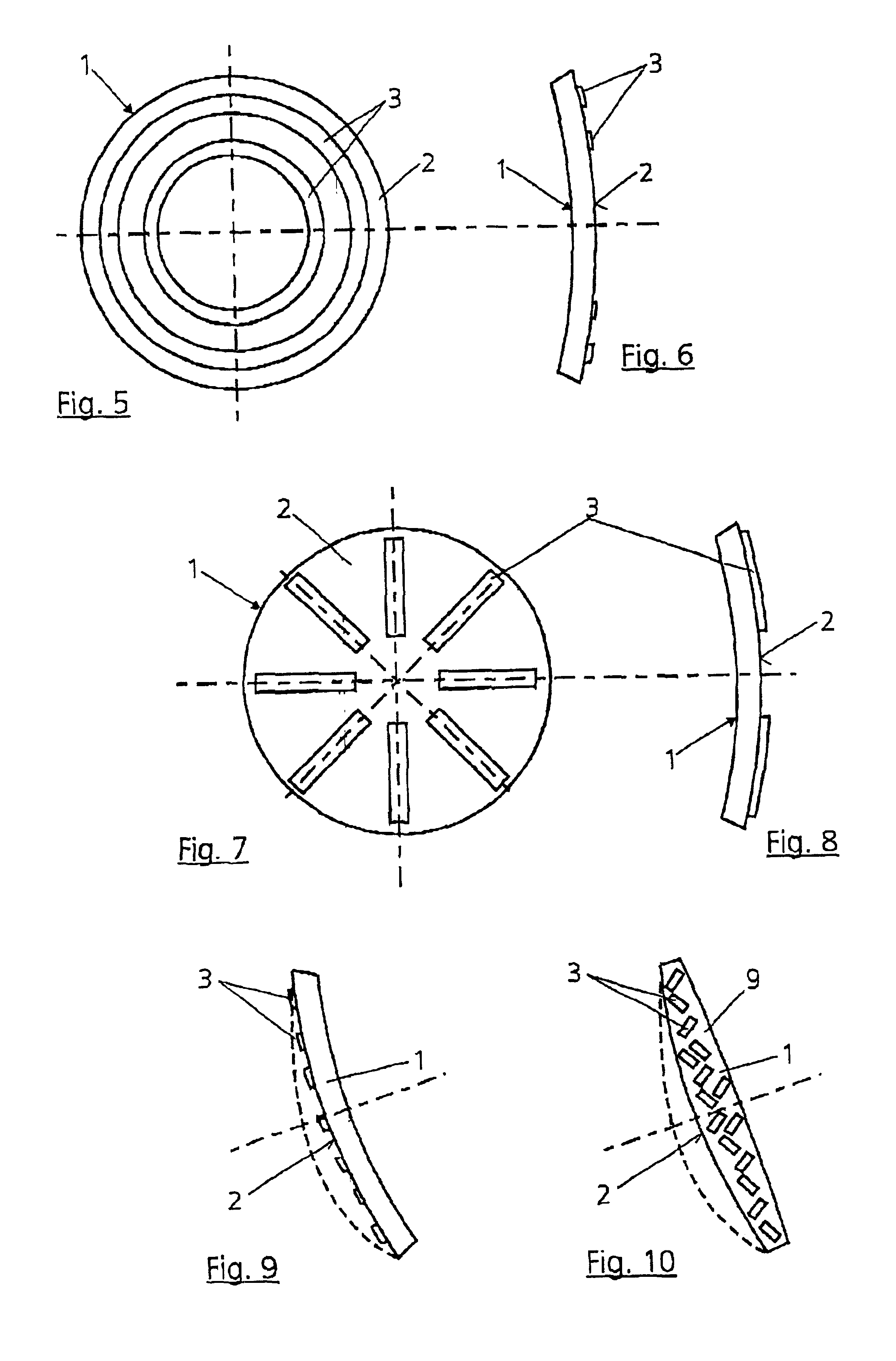
In accordance with FIG. 1, a mirror 1 is provided with piezoelectric elements 3 on its rear 2 as surface to be deformed. Two piezoelectric elements 3, which form the shape of a cross, are provided in accordance with the illustration.

Capacitive ranging sensors 4 at a short distance from the rear 2 are provided in order to detect the state of deformation. The piezoelectric elements 3 are piezoelectric ceramic films (PZT films) which are integrated in the mirror material or bonded onto the rear 2, and which can for example, have a thickness of a few μm. When the PZT films are being driven, they experience in accordance with the piezoelectric effect a strain which impresses forces on the mirror via the connection with the mirror substrate, and this leads to deformation of the mirror. Multifarious “patterns” are conceivable for generating any desired states of deformation in any desired angular orientation. As a rule, the piezoelectric elements will be provided for low corrugations, alth...


PUM

PropertyMeasurementUnit
forcesaaaaaaaaaa
piezoelectricaaaaaaaaaa
focal lengthaaaaaaaaaa

Abstract

In a system for specific deformation of optical elements in an imaging device, in particular in a projection exposure machine having a projection lens for micro-lithography, for the purpose of eliminating image errors or for active adjustment, piezoelectric elements are applied as actuators in the form of thin plates, films or layers to surfaces to be deformed, or integrated into them. In conjunction with an adaptronic servo loop having sensors, forces and / or moments are exerted on the optical elements for their specific deformation by means of a controlled activation of the piezoelectric elements as actuators.

Description

RELATED APPLICATIONSThis application relates to and claims priority to corresponding German Patent Application No. 100 46 379.7 filed on Sep. 20, 2000.BACKGROUND OF THE INVENTIONThe invention relates to an optical element deformation system in an imaging device for the purpose of eliminating image errors or for active adjustment.Very high imaging accuracies are required in many optical fields, in particular in micro-lithography. The aim is to minimize image errors even more. One of the main causes of image errors in this case is deformations of the optical elements. Such deformations can be introduced via mounts or be produced by mounts. Weight forces on optical elements can also lead to deformations and thus to image errors.Reference is made to WO 97 / 34171 in relation to the general prior art.Moreover, the precise adjustment of an imaging device, for example a projection lens, also requires individual optical elements to be actively adjusted in order, for example, to compensate err...

Claims


Application Information

Patent Timeline
Patent Type & Authority Patents(United States)
IPC IPC(8): G02B26/06G02B27/00G02B26/00G03F7/20G02B5/10G02B13/24G02B26/08G02B27/18H01L21/027
CPCG02B26/06G03F7/70258G02B27/0068G02B26/08
Inventor MELZER, FRANKMUHLBEYER, MICHAELGELLRICH, BERNHARDSORG, FRANZXALTER, STEFANITTNER, THOMAS
Owner CARL ZEISS SMT GMBH
Why Eureka
Try Eureka