
Method and apparatus for collecting and displaying bit-fail-map information

a technology of map information and display interface, applied in the direction of electronic circuit testing, emergency protective arrangements for automatic disconnection, instruments, etc., can solve the problems of not being able to test each chip individually, testing all the chips on the wafer, and lack of display interfa

Inactive Publication Date: 2005-01-18
POLARIS INNOVATIONS
View PDF4 Cites 15 Cited by
  • Summary
  • Abstract
  • Description
  • Claims
  • Application Information

AI Technical Summary

Benefits of technology

Disclosed is a method of testing memory, comprising providing one or more semiconductor wafers having one or more semiconductor chips thereon, each said chip comprising one or more segments, each said segment comprising one or more memory cells; providing a programmable testing apparatus comprising one or more test pattern generators and a test bed adapted to receive said one or more wafers in communicative contact so as to address individual memory cells, segments, chips, and wafers and transmit information thereto and receive information therefrom; receiving...

Problems solved by technology

The main drawback of such “front-end” systems is that they test all the chips on a wafer and are unable to test chips individually.
Another drawback is that they usually lack a display interface that permits pinpointing individual memory cell failures on individual chips or to allow the user to conveniently tailor memory tests to his own uses.

Method used


Image

  • Method and apparatus for collecting and displaying bit-fail-map information
  • Method and apparatus for collecting and displaying bit-fail-map information
  • Method and apparatus for collecting and displaying bit-fail-map information

Examples


Embodiment Construction

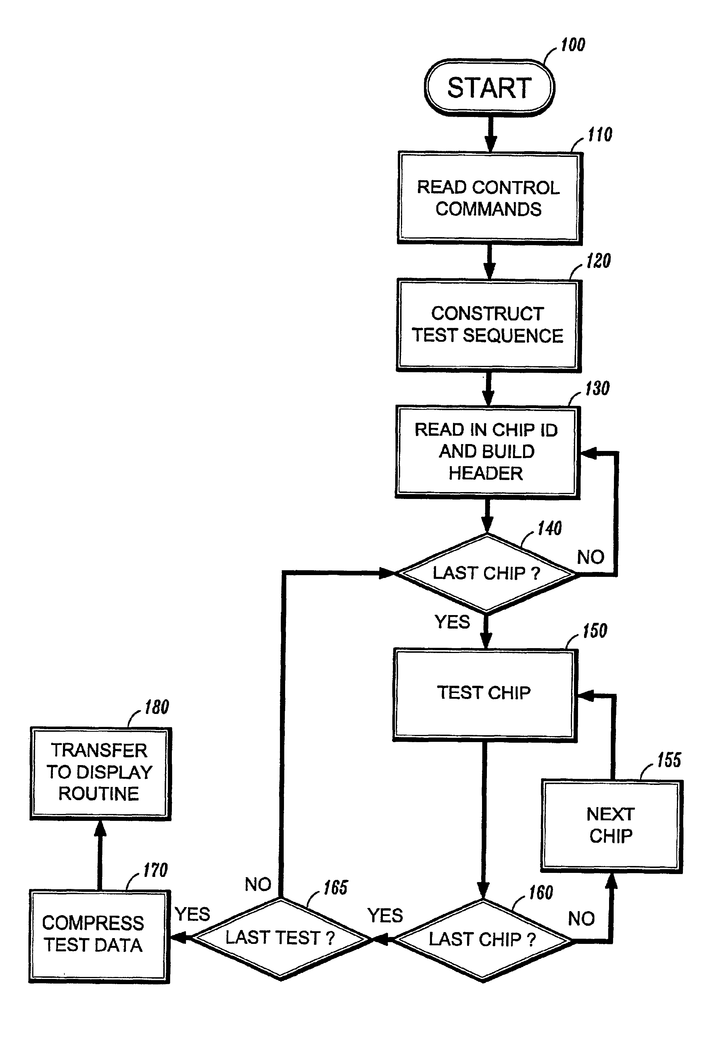
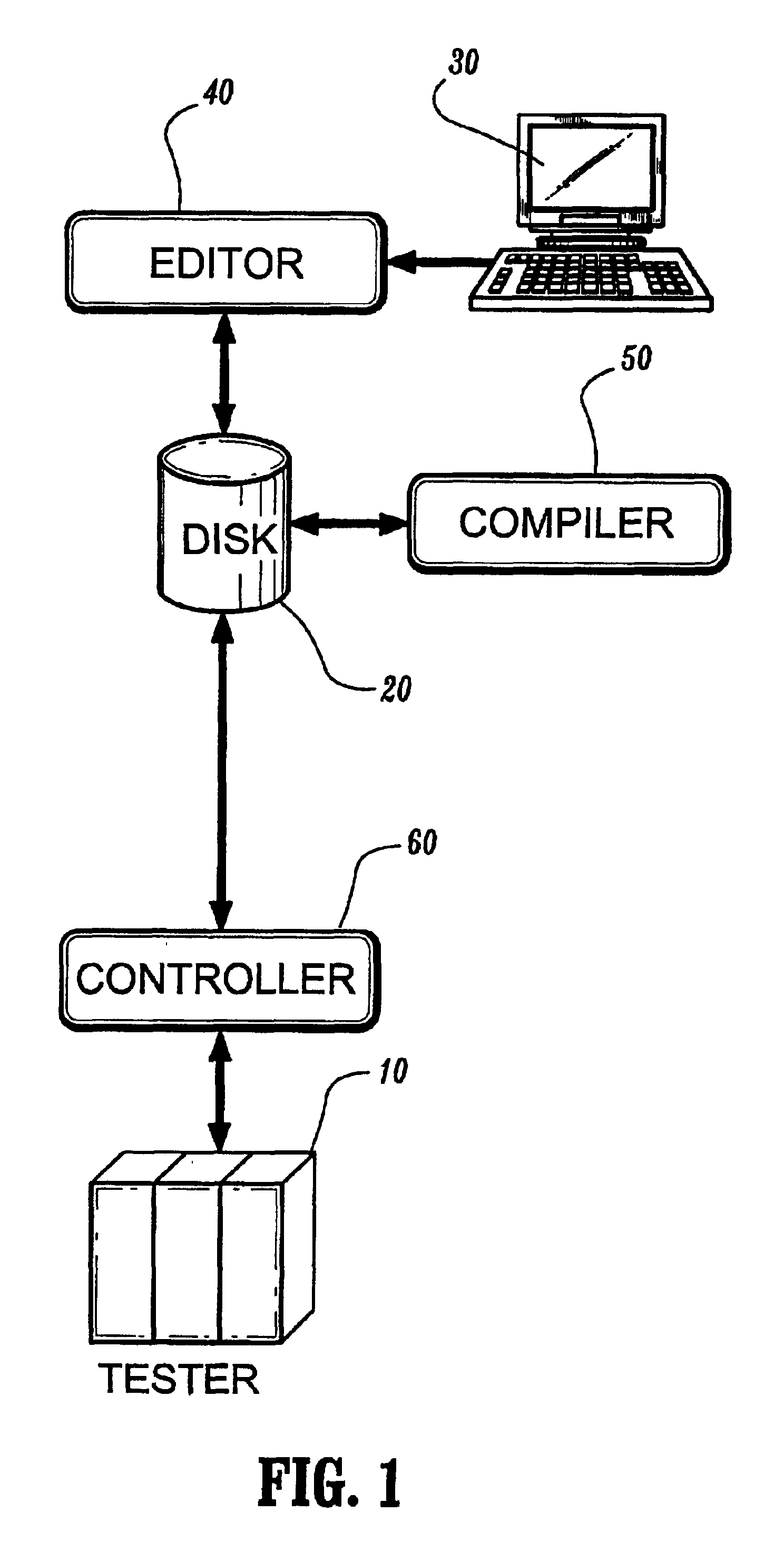
Referring to FIG. 1, there is shown an overview of an embodiment of the invention in which there is provided a memory tester 10 in communication, via a controller 60, with a viewing database on a storage medium 20 that is in turn in communication, either directly or via an editor 40, with a display device 30, such as a personal computer, workstation, or the like. The memory tester 10 is either linked to, or itself contains, an apparatus for executing programmable instructions, such as a central processing unit (CPU) and memory, or other device effective in executing the methods of this invention. An external compiler 50 may be provided where the tester 10 lacks compilation means. The external compiler 50 will generally be an apparatus for executing programmable instructions and may itself be part of a computer system that includes the display unit 30, an editor 40, and the database 20, or any combination thereof. A controller 60 controls communication between the storage medium 20 a...


PUM


Abstract

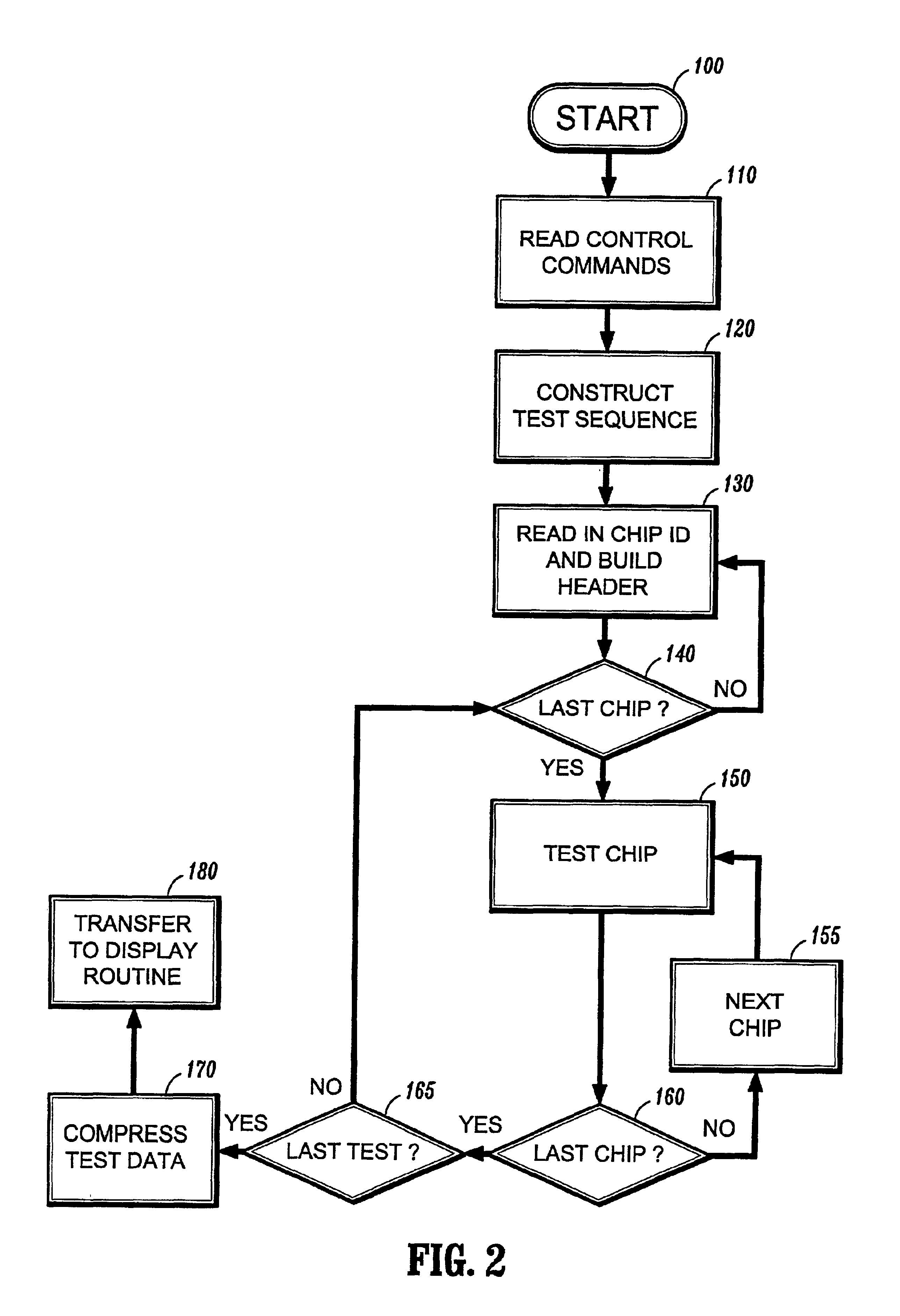
Disclosed is a method of testing memory, comprising providing one or more semiconductor wafers having one or more semiconductor chips thereon, each said chip comprising one or more memory cells, providing a programmable testing apparatus comprising at least one test pattern generators and a test bed adapted to receive said one or more wafers in communicative contact so as to address individual memory cells, chips, and wafers and transmit information thereto and receive information therefrom, receiving one or more test commands, constructing a test sequence of one or more commanded tests from said test commands, constructing at least one header comprising location information for each said wafer, chip and memory cell, testing said memory cells with a test pattern generated by said test pattern generator, collecting the results of said testing and passing them to a display device, passing said location information to said display device, constructing and displaying a graphical representation of said test results using said location information.

Description

BACKGROUND OF THE INVENTION1. Field of the InventionThis invention relates to a method and apparatus of testing memory arrays and displaying the test results.2. Discussion of the Related ArtIn the manufacture of semiconductor wafers having multiple memory chips, or “chips” thereon it is known to “front-end” test the entire wafer to ensure the memory is functioning correctly. Memory testers sold under the “Advantest” mark, will usually have software available for this purpose. Advantest has available a software program sold under the tradename “AQUA”, which is compatible with most later models of Advantest-brand memory testers, though not the earlier models. The main drawback of such “front-end” systems is that they test all the chips on a wafer and are unable to test chips individually. Another drawback is that they usually lack a display interface that permits pinpointing individual memory cell failures on individual chips or to allow the user to conveniently tailor memory tests to...

Claims


Application Information

Patent Timeline
IPC IPC(8): G11C29/56G09G5/38
CPCG11C29/56
Inventor LUONG, JIMMY BA
Owner POLARIS INNOVATIONS
Learn More