Boron phosphide-based semiconductor layer and vapor phase growth method thereof

a technology of boron phosphide and semiconductor layer, which is applied in the direction of crystal growth process, polycrystalline material growth, chemically reactive gas growth, etc., can solve the problems of low forward voltage (vf) and poor rectification characteristics of led, and achieve excellent surface flatness and continuity

Inactive Publication Date: 2005-01-25
SHOWA DENKO KK
View PDF5 Cites 5 Cited by
  • Summary
  • Abstract
  • Description
  • Claims
  • Application Information

AI Technical Summary

Benefits of technology

The present invention aims to solve problems in the prior art by providing a method for growing a boron-phosphide-based semiconductor layer on a single-crystal silicon substrate that has excellent surface flatness and continuity. The invention suppresses the release of substances that impair the formation of the semiconductor layer from decomposition products deposited on the inner wall of a vapor-phase growth reactor.

Problems solved by technology

The patent text describes a problem with a boron-phosphide-based semiconductor layer formed on a single-crystal silicon substrate that has a rough surface and contains discontinuities. This is caused by the formation of a silicon nitride film or silicon dioxide film as a masking material to prevent growth of a nitrogen-containing Group III nitride semiconductor layer. The technical problem is to provide a method for forming a continuous crystal layer on the surface of a single-crystal silicon substrate that has been solved through a vapor-phase growth reactor.

Method used


Image

  • Boron phosphide-based semiconductor layer and vapor phase growth method thereof
  • Boron phosphide-based semiconductor layer and vapor phase growth method thereof
  • Boron phosphide-based semiconductor layer and vapor phase growth method thereof

Examples


first embodiment

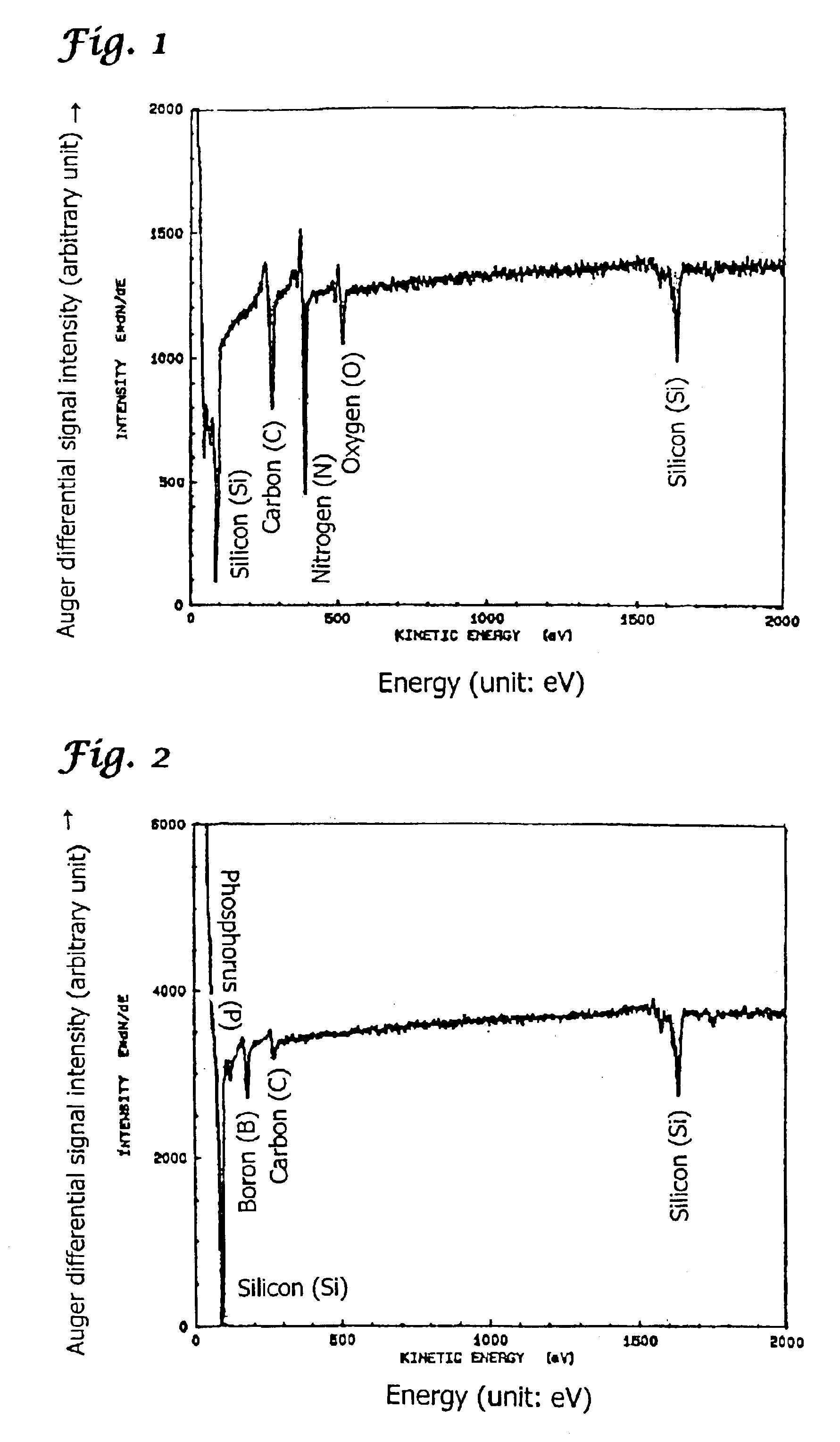
In the present invention, before the aforementioned single-crystal silicon substrate is mounted on a susceptor, the inner wall of a vapor-phase growth reactor formed of, for example, quartz, stainless steel, or a ceramic material such as boron nitride (BN), is covered with a film containing boron and phosphorus. The expression “the inner wall of a vapor-phase growth reactor” refers to the inner walls constituting the reactor that face the substrate. Specifically, the aforementioned film is formed by feeding into the vapor-phase growth reactor a boron-containing gas, a phosphorus-containing gas, and a carrier gas for carrying these gases, while the susceptor formed of a heat-resistant material such as graphite or silicon carbide (SiC) is maintained at a temperature of 500° C. to 1,200° C. The thus-formed film covers a layer of nitrogen (N)-containing decomposition products deposited onto the inner wall of the vapor-phase growth reactor.

Examples of the boron-containing gas include tri...

examples

Example of the Invention

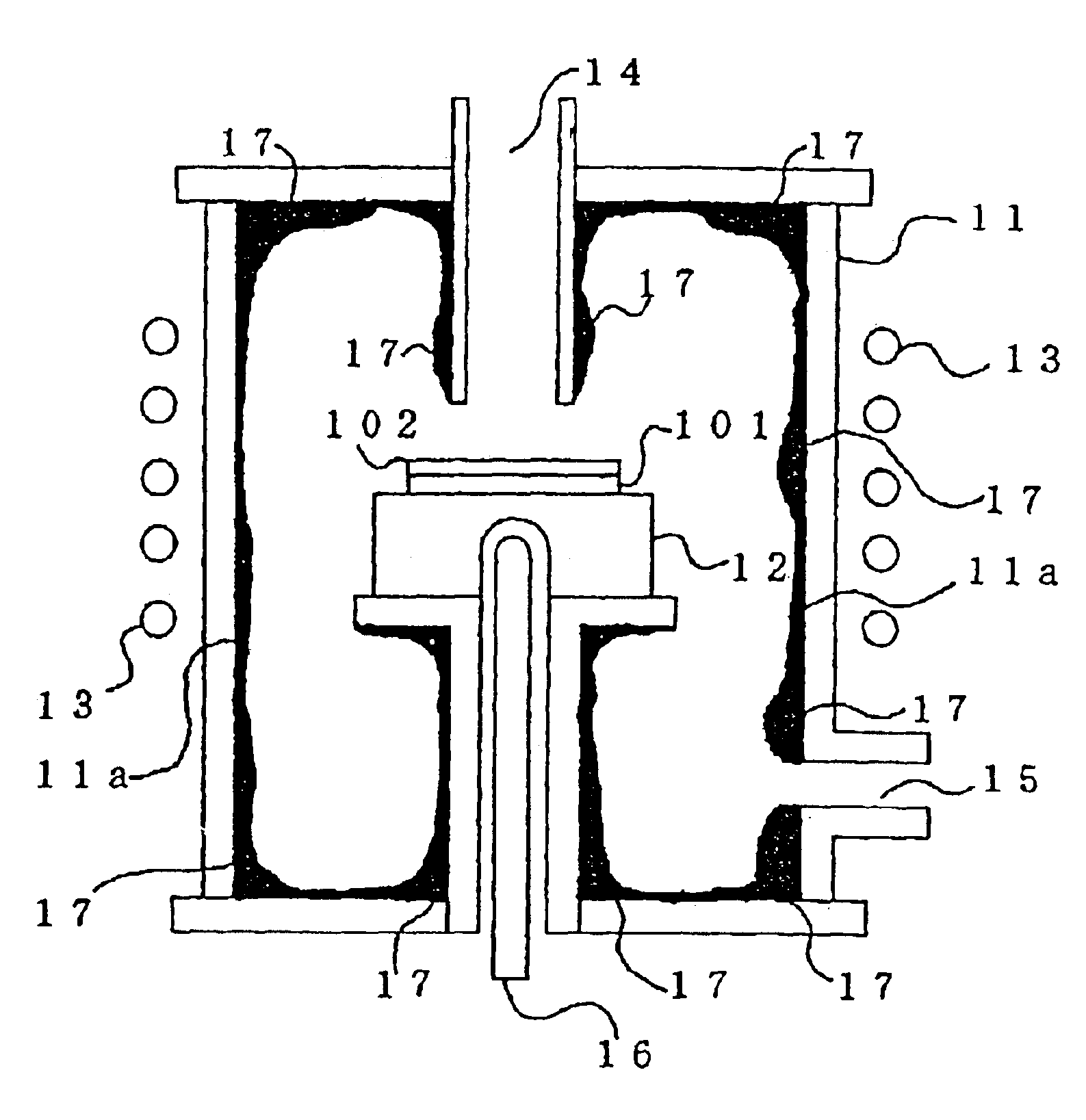
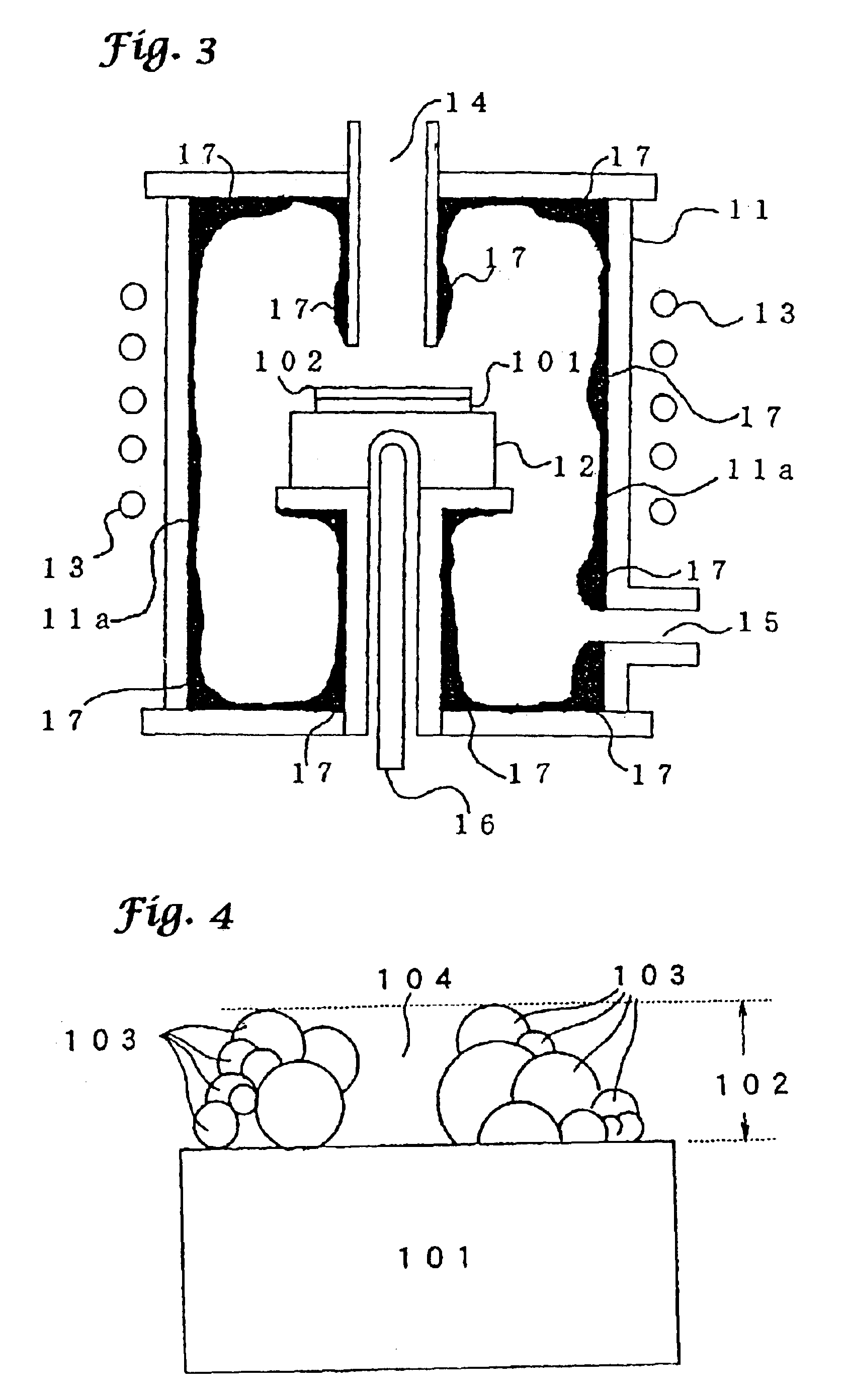
The present invention will now be described in detail by taking, as an example, the case where a boron monophosphide layer is vapor-grown directly on the surface of a boron-doped p-type single-crystal silicon substrate having a {111} crystal plane through MOCVD. FIG. 3 schematically shows the structure of an MOCVD vapor-phase growth apparatus employed in the present Example.

A vapor-phase growth reactor 11 of the vapor-phase growth apparatus shown in FIG. 3 is formed of a high-purity quartz tube for use in the semiconductor industry. In the center of the cylindrical vapor-phase growth reactor 11, a columnar susceptor 12 formed of high-purity graphite is provided for placing a substrate thereon. A high-frequency coil 13 for effecting high-frequency induction heating of the susceptor 12 is provided around the outer wall of the vapor-phase growth reactor 11 that is located in the vicinity of the susceptor 12. On an end of the vapor-phase growth reactor 11, an inl...


PUM


Abstract

A vapor-phase growth method for forming a boron-phosphide-based semiconductor layer on a single-crystal silicon (Si) substrate in a vapor-phase growth reactor. The method includes preliminary feeding of a boron (B)-containing gas, a phosphorus (P)-containing gas, and a carrier gas for carrying these gases into a vapor-phase growth reactor to thereby form a film containing boron and phosphorus on the inner wall of the vapor-phase growth reactor; and subsequently vapor-growing a boron-phosphide-based semiconductor layer on a single-crystal silicon substrate. Also disclosed is a boron-phosphide-based semiconductor layer prepared by the vapor-phase growth method.

Description


Claims


Application Information

Patent Timeline
Owner SHOWA DENKO KK
Why Eureka
Try Eureka