Transmission circuit and radio transmission apparatus
- Summary
- Abstract
- Description
- Claims
- Application Information
AI Technical Summary
Benefits of technology
Problems solved by technology
Method used
Image

Examples
first embodiment
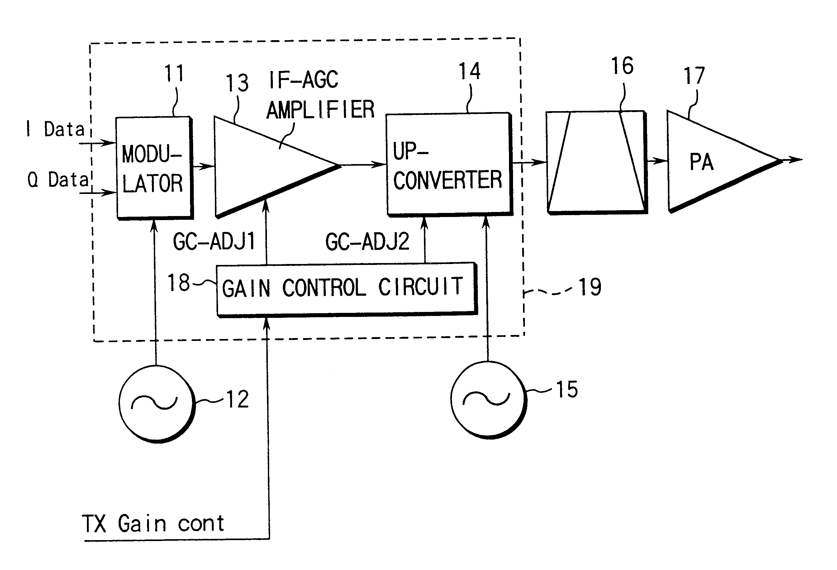
FIG. 2 is a block diagram showing a transmission apparatus wherein this invention is applied to a CDMA mobile telephone.
An I-phase transmission data signal I-DATA and a Q-phase transmission data signal Q-DATA are output from a data processor (not shown in FIG. 2) provided in the mobile telephone. The I-phase transmission data signal I-DATA and the Q-phase transmission data signal Q-DATA, which are spread-spectrum processed and have an orthogonal relationship to each other, are input to a modulator 11. A TX-IF local oscillator (intermediate frequency signal generating circuit) 12 outputs an intermediate frequency local oscillator signal to the modulator 11.
The modulator 11 modulates the intermediate frequency local oscillator signal output from the TX-IF local oscillator 12 in accordance with the orthogonal transmission data signals I-DATA and Q-DATA.
The modulator 11 delivers a modulated signal to an IF-AGC amplifier (intermediate frequency gain control amplifier) 13. The IF-AGC amp...
second embodiment
Subsequently, the invention will be explained.
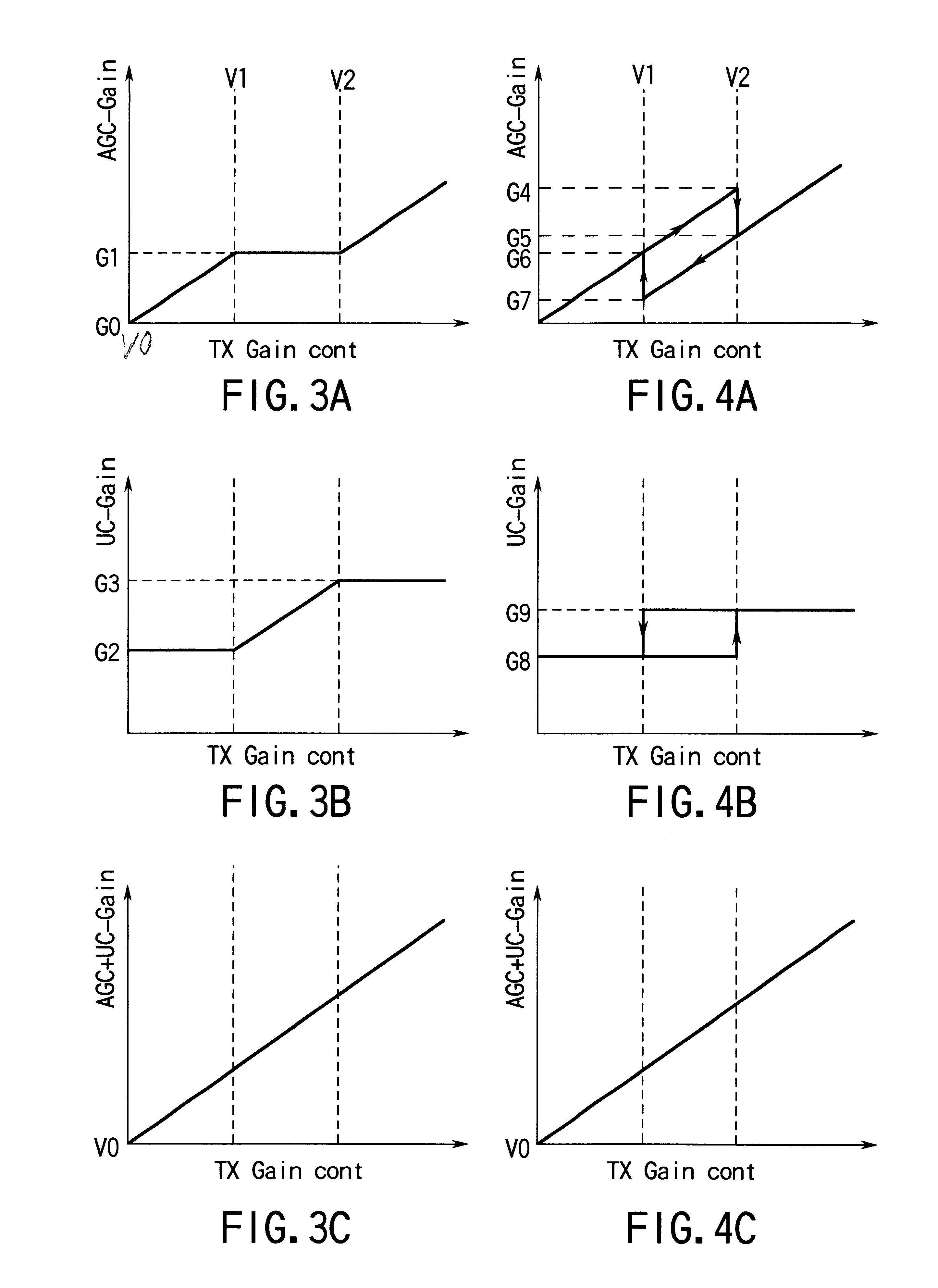
The block constitution of the transmission apparatus according to the second embodiment is identical to that shown in FIG. 2, with the exception that the method for generating the gain adjustment signals GC-ADJ1 and GC-ADJ2 in the gain control circuit 18 differs from that in the case shown in FIG. 2. Therefore, only those points which differ from FIG. 2 will be explained below with reference to FIGS. 4A to 4C.
When the voltage level of the gain control signal TX Gain cont. input to the gain control circuit 18 changes from V0 to the other threshold value V2, the gain control circuit 18 generates the gain adjustment signal GC-ADJ1 so that the gain AGC-Gain of the IF-AGC amplifier 13 increases linearly (monotonously) from G0 to G4 while passing G6 as shown in FIG. 4A. In addition, the gain control circuit 18 generates the other gain adjustment signal GC-ADJ2 so that the gain UC-Gain of the up-converter 14 remains constant at G8 as shown in F...
PUM
 Abstract
Description
Claims
Application Information