Integrated circuit die and an electronic assembly having a three-dimensional interconnection scheme

a technology of integrated circuits and electronic assemblies, applied in the field of electronic assemblies, can solve problems such as metal lines in substrates, and inability to achieve the effect of reducing the number of components

Inactive Publication Date: 2005-02-01
INTEL CORP
View PDF109 Cites 89 Cited by
  • Summary
  • Abstract
  • Description
  • Claims
  • Application Information

AI Technical Summary

Problems solved by technology

In other applications, the metal lines in substrates may inhibit performance.
These techniques are in some respects undesirable, because they require etching of an opening in a die.
All of these factors contribute to limiting throughput.

Method used


Image

  • Integrated circuit die and an electronic assembly having a three-dimensional interconnection scheme
  • Integrated circuit die and an electronic assembly having a three-dimensional interconnection scheme
  • Integrated circuit die and an electronic assembly having a three-dimensional interconnection scheme

Examples


Embodiment Construction

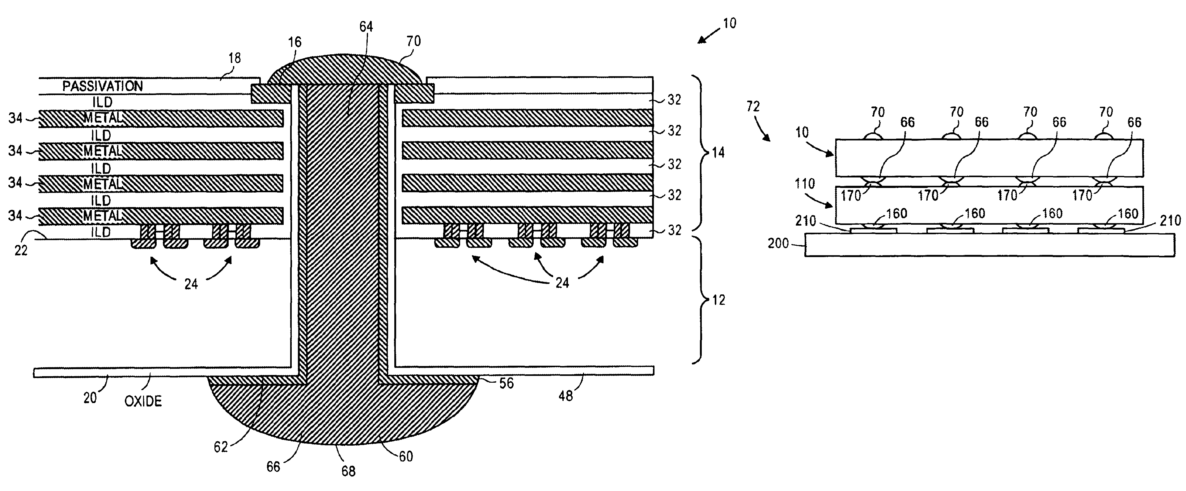
The following description relates to the construction of an electronic assembly by stacking two or more integrated circuit dies on top of one another. An opening is laser-drilled into an upper die, and subsequently filled with a conductive member. The conductive member is located on a lower die and interconnects integrated circuits of the upper and lower dies. Laser-drilling allows for faster throughput when compared to, for example, etching, especially if a smaller number of openings has to be formed. The opening is laser-drilled from an upper surface of the upper die all the way through the die, which allows for the use of alignment marks on an upper surface of the upper die.

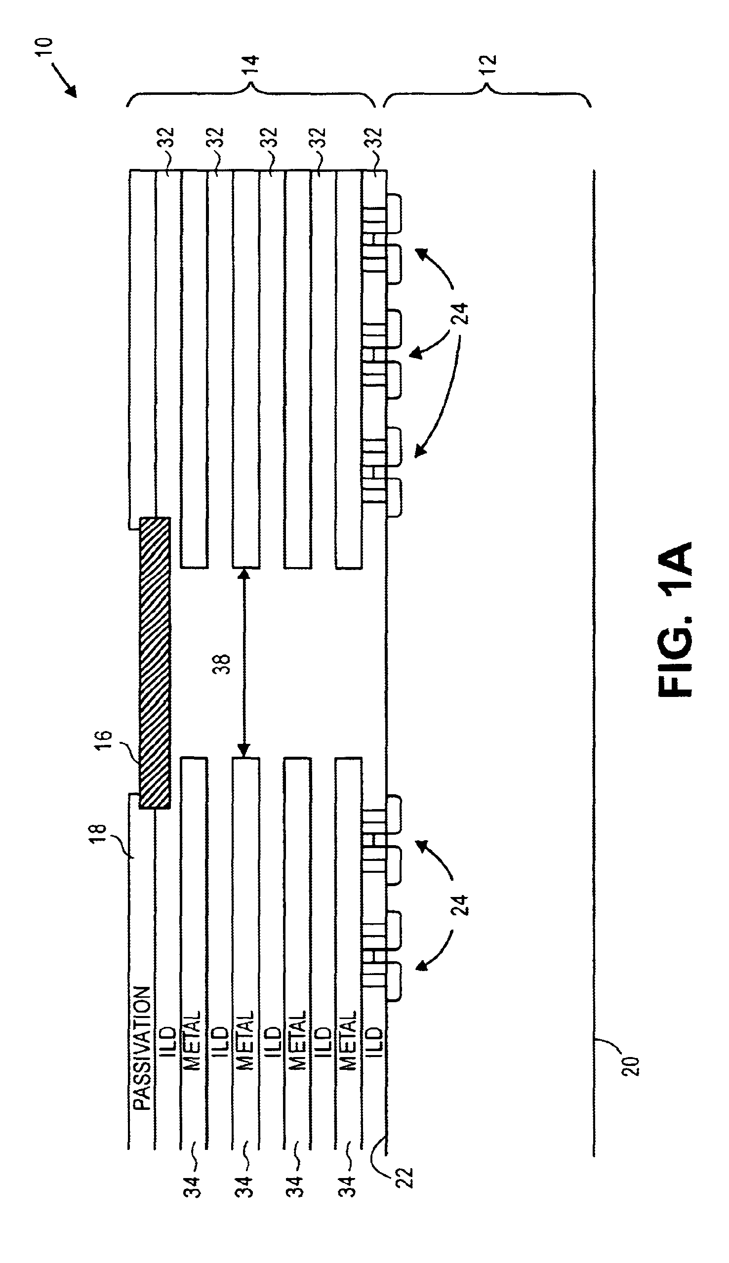
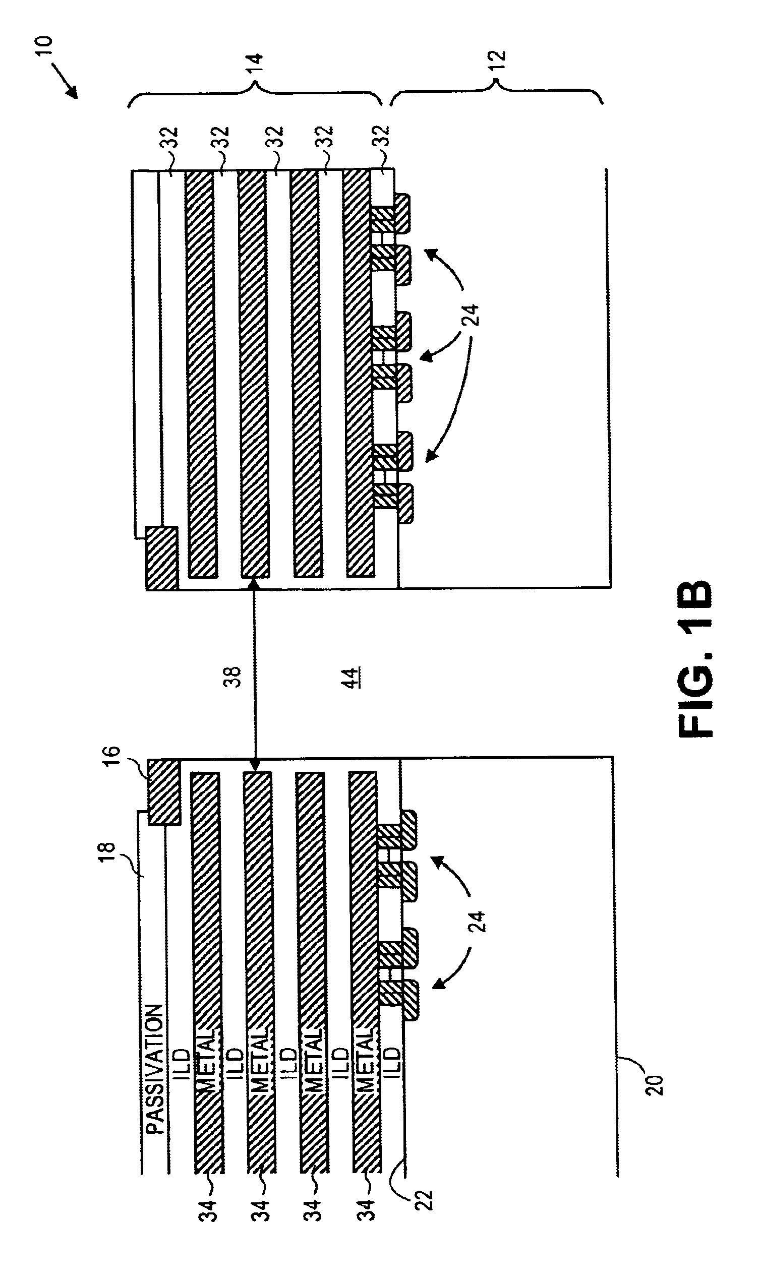
Referring now to FIG. 1A, a portion of a fabricated wafer is shown, including a die 10 having a silicon substrate 12 and an integrated circuit 14 formed on the silicon substrate 12. The die 10 further includes a contact pad 16 and a passivation layer 18.

The silicon substrate 12 has a lower surface 20 and an up...


PUM

PropertyMeasurementUnit
wavelengthaaaaaaaaaa
diameteraaaaaaaaaa
diameteraaaaaaaaaa

Abstract

An electronic assembly is assembled by stacking two or more integrated circuit dies on top of one another. Prior to singulation, an opening is laser-drilled into an upper die, and subsequently filled with a conductive member. The conductive member is located on a lower die and interconnects integrated circuits of the upper and lower dies. Laser-drilling allows for faster throughput when compared to, for example, etching, especially if a small number of openings has to be formed. The opening is laser-drilled from an upper surface of the upper die all the way through the die, which allows for the use of alignment marks on an upper surface of the upper die.

Description

BACKGROUND OF THE INVENTION1. Field of the InventionThis invention relates to an electronic assembly of the kind having a plurality of integrated circuit dies stacked onto one another, and its manufacture.2. Discussion of Related ArtIn conventional computer assemblies, integrated circuits are “two-dimensionally” connected to one another. Two dies may, for example, be mounted to a common substrate having metal lines that interconnect the integrated circuits of the dies with one another. A “three-dimensional” interconnection scheme may in certain instances be more desirable. Handheld devices may, for example, require a more compact packaging arrangement. In other applications, the metal lines in substrates may inhibit performance. Other applications may also require a three-dimensional interconnection scheme to allow for the design of more sophisticated, three-dimensional logic.Some techniques for forming contacts on a substrate side of a die are disclosed in U.S. Pat. No. 6,184,060. ...

Claims


Application Information

Patent Timeline
Patent Type & Authority Patents(United States)
IPC IPC(8): H01L25/065H01L21/70H01L23/48H01L21/768
CPCH01L21/76898H01L23/481H01L25/0657H01L25/50H01L2225/06513Y10T29/49155H01L2225/06541H01L2225/06589H01L2224/16Y10T29/49165H01L2225/06517
Inventor SWAN, JOHANNA M.NATARAJAN, BALACHIANG, CHIENATWOOD, GREGRAO, VALLURI R.
Owner INTEL CORP
Why Eureka
Try Eureka