Packaging microelectromechanical structures

a micro-electromechanical and packaging technology, applied in the field of packaging micro-electromechanical structures, can solve the problems of increasing the size of the resulting product, affecting the reliability of the method, and affecting the accuracy of the product,

Inactive Publication Date: 2005-02-08
INTEL CORP
View PDF9 Cites 117 Cited by
  • Summary
  • Abstract
  • Description
  • Claims
  • Application Information

AI Technical Summary

Problems solved by technology

This approach, while reliable, may be cost prohibitive for many commercial applications.
However, this technique requires high temperature bonding that may not be suitable for all components utilized in some MEMS applications.
In some cases, the glass frit occupies a l

Method used


Image

  • Packaging microelectromechanical structures
  • Packaging microelectromechanical structures
  • Packaging microelectromechanical structures

Examples


Embodiment Construction

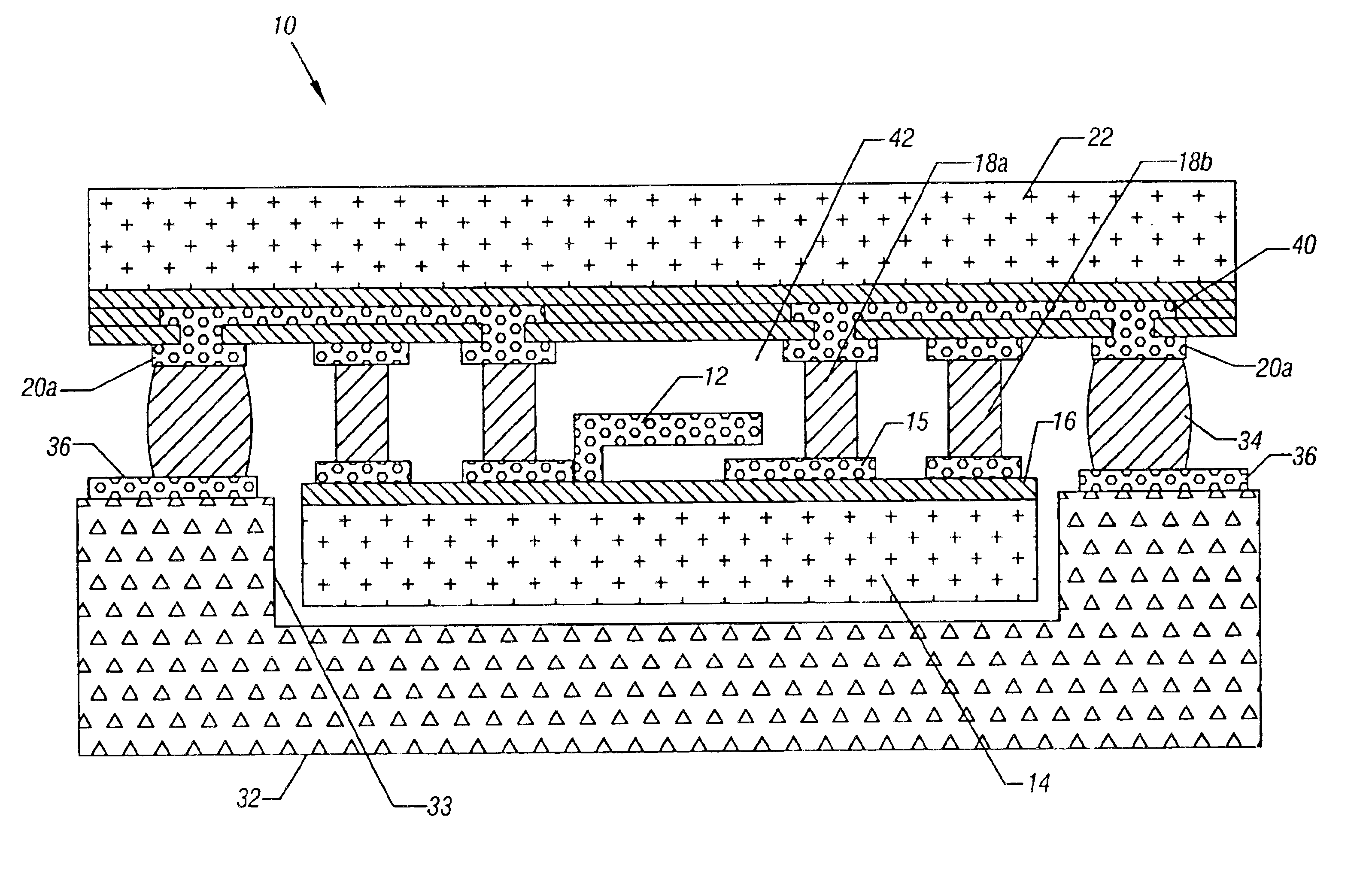
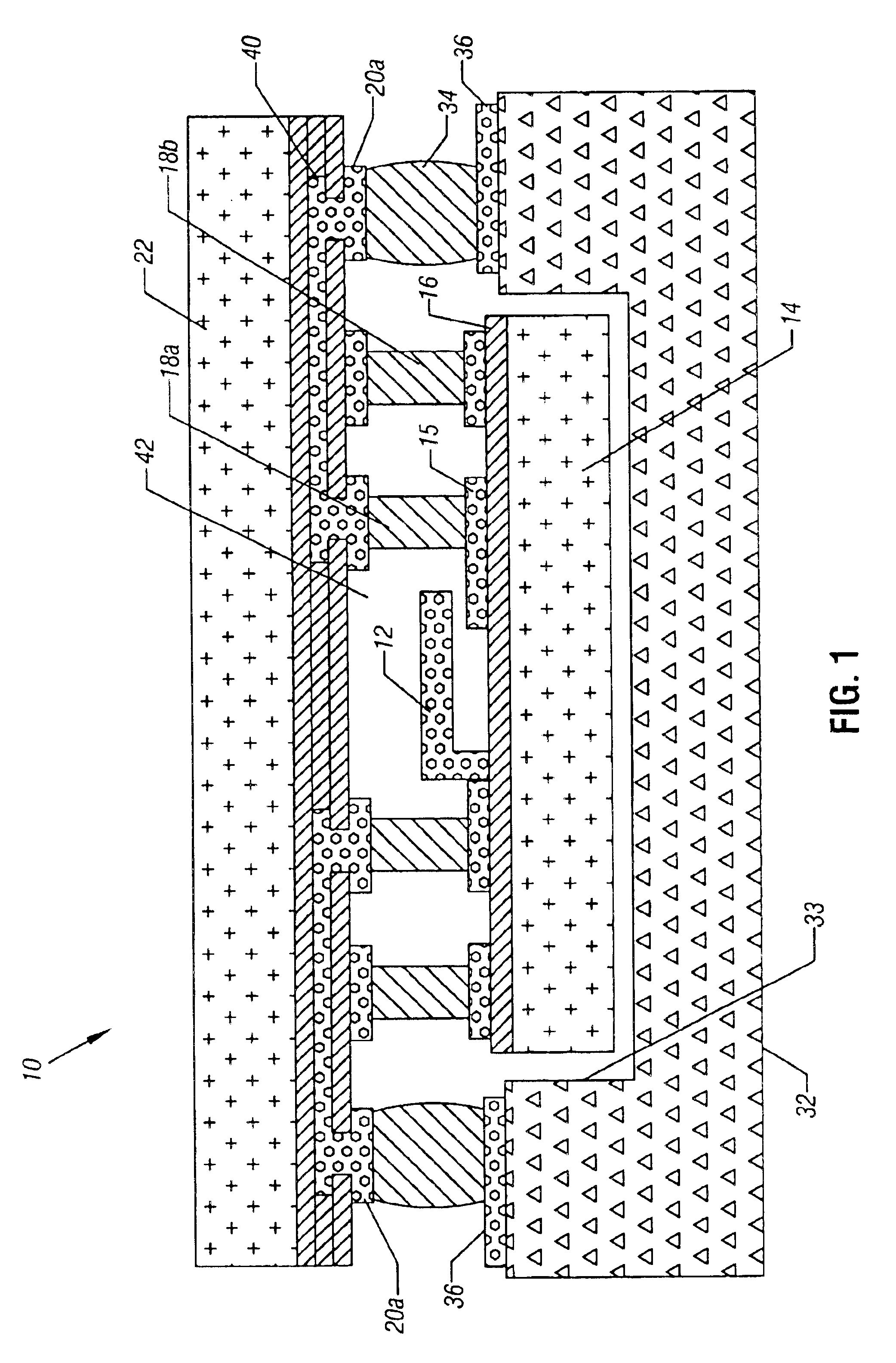
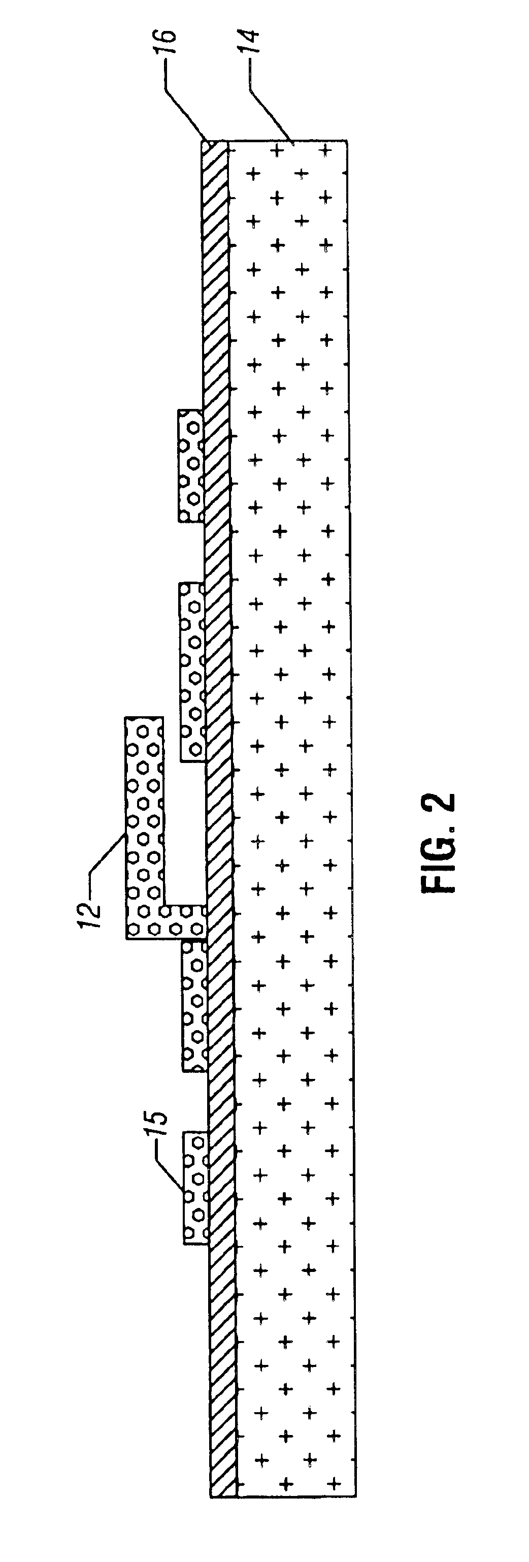
Referring to FIG. 1, a MEMS component 12, such as a radio frequency (RF) MEMS component, including as examples a varactor, a switch or a resonator, may be formed on a semiconductor structure 14 having a layer 16. A plurality of bond pads 15 and 16 may be provided on the layer 16. The MEMS component 12 may be surrounded on one side by a printed circuit board 32 having a cavity 33 conforming to the shape of the semiconductor structure 14 in some embodiments. A gap may be maintained between the board 32 and the structure 14.

A plurality of solder bumps 34 may bond the printed circuit board 32 to a semiconductor structure 22 through bond pads 36 and 20a. The semiconductor structure 22 may have internal electrical interconnection layers 40 that interconnect bond pads 15, 20a and 36 on the structure 14, the board 32 and the semiconductor structure 22. Thus, electrical connections are possible between the various components.

A solder ring 18b completely encircles the MEMS device 12, defining...


PUM


Abstract

A MEMS device may be formed in a hermetic cavity by sealing a pair of semiconductor structures to one another, enclosing the MEMS device. The two structures may be coupled using surface mount techniques as one example, so that the temperatures utilized may be compatible with many MEMS applications. Electrical interconnection layers in one or the other of these structures may be utilized to allow electrical interconnections from the exterior world to the MEMS components within the cavity.

Description

BACKGROUNDThis invention relates generally to microelectromechanical structures (MEMS) and particularly to techniques for packaging MEMS.In some cases, MEMS components such as varactors, switches and resonators need to be packaged in a hermetic environment. For example, particularly with radio frequency MEMS components, there may be a need for hermetic packaging. Such packaging protects the MEMS components from the outside environment.Conventionally, two approaches have been utilized for hermetic packaging of MEMS components. Ceramic packages with cavities that may be sealed are used in the defense industry. This approach, while reliable, may be cost prohibitive for many commercial applications.A second approach is to use a glass frit to bond a wafer containing the MEMS components to a cover. However, this technique requires high temperature bonding that may not be suitable for all components utilized in some MEMS applications. In some cases, the glass frit occupies a large area tha...

Claims


Application Information

Patent Timeline
IPC IPC(8): B81B7/00H01L23/02H01L23/10
CPCB81B7/0006H01L23/10H01L2924/01079H01L2224/16H01L2924/1461H01L2924/00H01L2224/05573H01L2224/05568H01L2224/05572H01L2224/05567
Inventor MA, QINGRAO, VALLURIHECK, JOHNWONG, DANIELBERRY, MICHELE
Owner INTEL CORP
Why Eureka
Try Eureka