
Non-volatile memory with test rows for disturb detection

a non-volatile memory and test row technology, applied in static storage, digital storage, instruments, etc., can solve the problems of time-consuming and laborious process of checking the memory cells, voltage can disturb the memory cells in the un-selected blocks, and disturb the situation

Inactive Publication Date: 2005-02-08
MICRON TECH INC
View PDF32 Cites 79 Cited by
  • Summary
  • Abstract
  • Description
  • Claims
  • Application Information

AI Technical Summary

Problems solved by technology

These erase voltages can disturb the memory cells in the un-selected blocks.
A time consuming process of checking the memory cells in the un-selected blocks is typically performed to identify cells that required repair.
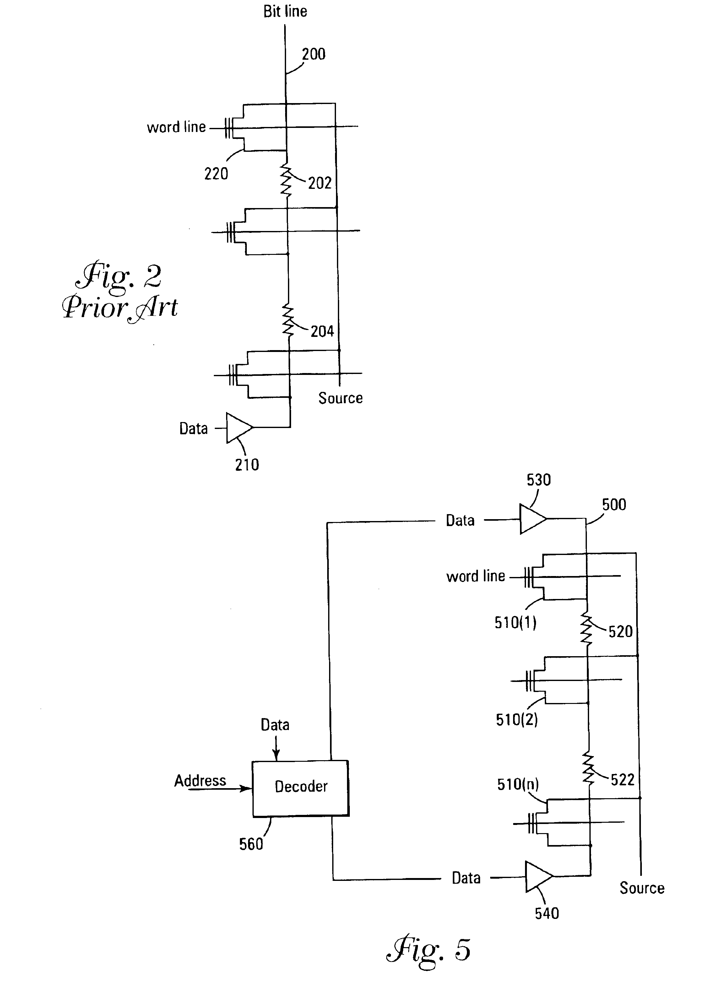
In a memory where common bit lines are shared across erase blocks, this positive voltage will create a disturb situation.

Method used


Image

  • Non-volatile memory with test rows for disturb detection
  • Non-volatile memory with test rows for disturb detection
  • Non-volatile memory with test rows for disturb detection

Examples


Embodiment Construction

In the following detailed description of the preferred embodiments, reference is made to the accompanying drawings that form a part hereof, and in which is shown by way of illustration specific preferred embodiments in which the inventions may be practiced. These embodiments are described in sufficient detail to enable those skilled in the art to practice the invention, and it is to be understood that other embodiments may be utilized and that logical, mechanical and electrical changes may be made without departing from the spirit and scope of the present invention. The following detailed description is, therefore, not to be taken in a limiting sense, and the scope of the present invention is defined only by the claims.

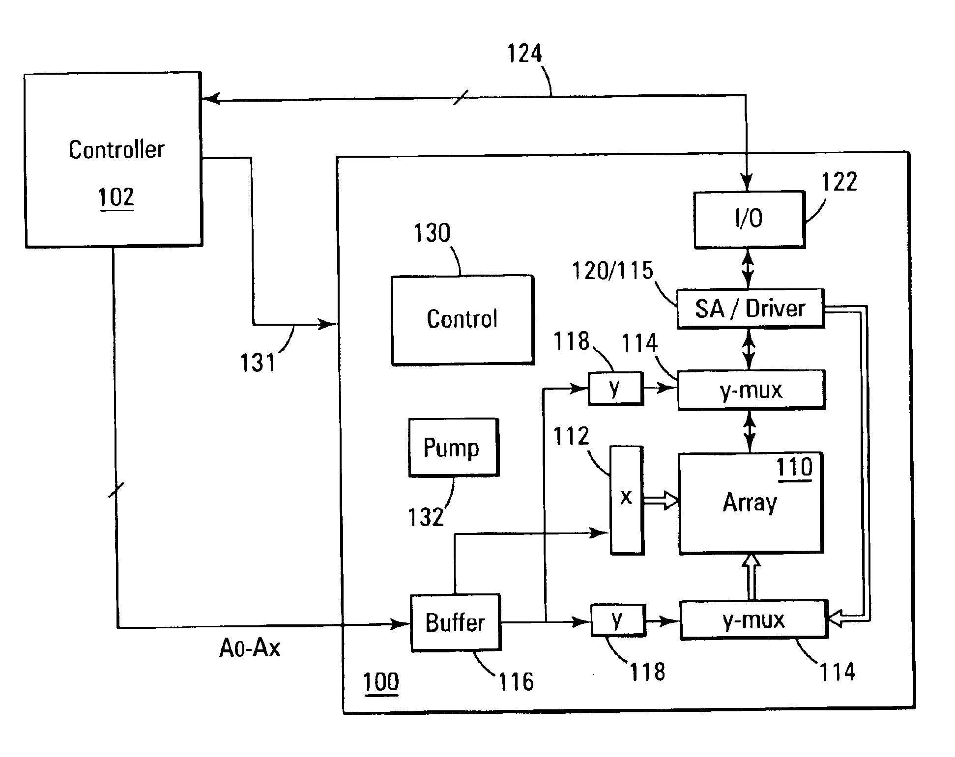
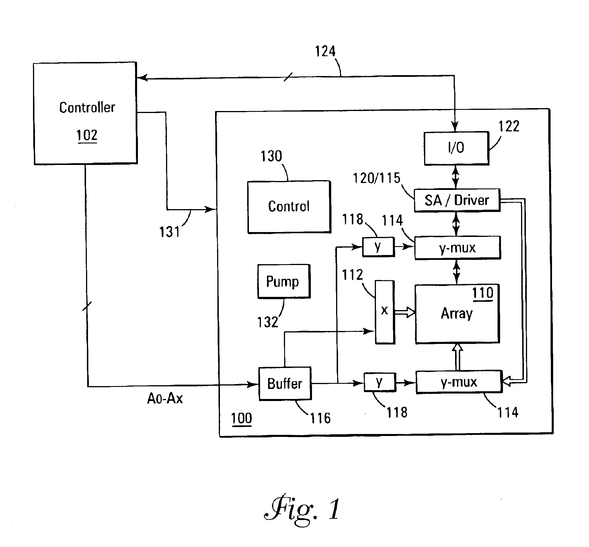
FIG. 1 illustrates a block diagram of a flash memory device 100 that is coupled to a controller 102. The memory device has been simplified to focus on features of the memory that are helpful in understanding the present invention. The memory device includes an array o...


PUM


Abstract

A non-volatile memory device has an array of memory cells arranged in rows and columns. The memory cells can be externally accessed for programming, erasing and reading operations. Test rows of memory cells are provided in the array to allow for memory cell disturb conditions. The test rows are not externally accessible for standard program and read operations. The test rows are located near bit line driver circuitry to insure the highest exposure to bit line voltages that may disturb memory cells in the array.

Description

TECHNICAL FIELD OF THE INVENTIONThe present invention relates generally to memory devices and in particular the present invention relates to non-volatile memory devices and leakage detection.BACKGROUND OF THE INVENTIONElectrically erasable and programmable read only memories (EEPROMs) are reprogrammable non-volatile memories that are widely used in computer systems for storing data. The typical data storage element of an EEPROM is a floating gate transistor, which is a field-effect transistor (FET) having an electrically isolated (floating) gate that controls electrical conduction between source and drain regions. Data is represented by charge stored on the floating gate and the resulting conductivity obtained between source and drain regions.For example, a floating gate memory cell can be formed in a P-type substrate with an N-type diffused source region and an N-type drain diffusion formed in the substrate. The spaced apart source and drain regions define an intermediate channel r...

Claims


Application Information

Patent Timeline
Patent Type & Authority Patents(United States)
IPC IPC(8): G11C16/34G11C16/06G11C29/24G11C29/04
CPCG11C16/3418G11C29/52G11C16/3445G11C29/24G11C16/3427G11C16/04
Inventor CHEVALLIER, CHRISTOPHE J.
Owner MICRON TECH INC
Learn More