Fabrication method of an electrostatic discharge protection circuit with a low resistant current path

a protection circuit and resistance current technology, applied in the direction of electrical equipment, semiconductor devices, semiconductor/solid-state device details, etc., can solve the problems of electrostatic discharge protection circuit failure, failure of integrated circuit, damage to the integrated circuit of the chip, etc., and achieve enhanced protection performance of the electrostatic discharge protection circuit

Inactive Publication Date: 2005-02-15
UNITED MICROELECTRONICS CORP
View PDF6 Cites 7 Cited by
  • Summary
  • Abstract
  • Description
  • Claims
  • Application Information

AI Technical Summary

Benefits of technology

The invention provides a structure and a fabrication method of an electrostatic discharge protection circuit, by which the protection performance of the electrostatic discharge protection circuit is enhanced.
The invention further provides a structure and a fabrication method of an electrostatic discharge protection circuit, by which the heat dissipation performance of the electrostatic discharge protection circuit is improved.
According to the above, in the electrostatic discharge protection circuit, a buried layer and a sinker layer electrically connected to the drain and the buried layer are formed. When the electrostatic discharge protection circuit is activated, the current flows in the substrate from the source through the buried layer and the sinker layer to the drain. Therefore, a large current flowing through a surface of the gate dielectric layer is prevented. Further, the gate dielectric layer is prevented from being blown. As a result, the dielectric strength of the electrostatic discharge protection circuit is increased, and the protection effect is enhanced.
Further, as the current flows in the substrate through the path from the source, the buried layer, the sinker layer to the drain, the thermal energy generated thereby is effectively dissipated. The heat dissipation performance of the electrostatic discharge protection circuit is significantly enhanced.

Problems solved by technology

The surge caused by such electrostatic discharge may damage the integrated circuit of the chip or even cause failure of the integrated circuit.
A large thermal energy may blow the gate dielectric to cause failure of the electrostatic discharge protection circuit.

Method used


Image

  • Fabrication method of an electrostatic discharge protection circuit with a low resistant current path
  • Fabrication method of an electrostatic discharge protection circuit with a low resistant current path
  • Fabrication method of an electrostatic discharge protection circuit with a low resistant current path

Examples


Embodiment Construction

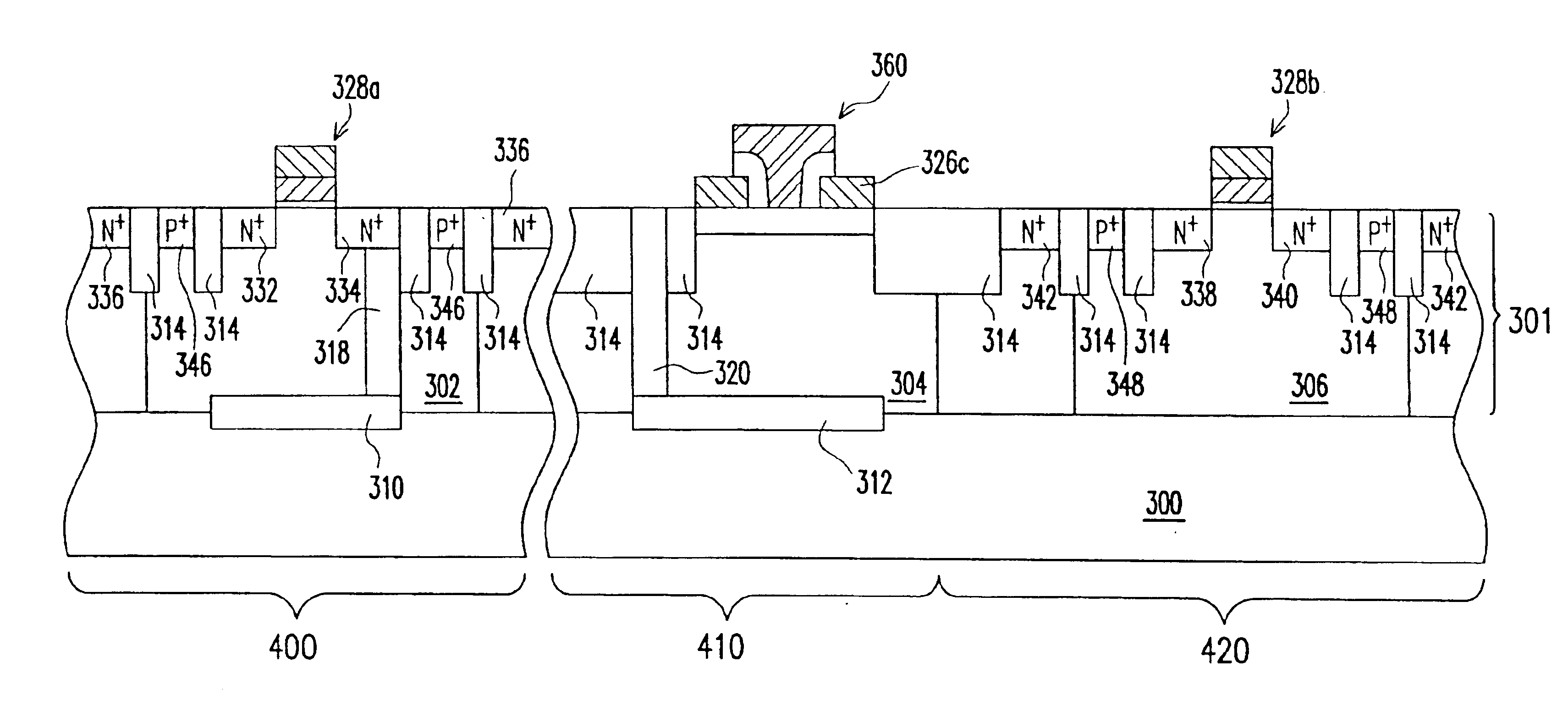
FIG. 3A shows a top view of an electrostatic discharge protection circuit in one embodiment of the invention, while FIG. 3B shows a cross-sectional view thereof.

Referring to FIG. 3A and FIG. 3B, the electrostatic discharge protection circuit provided by the invention includes a substrate 200, a well 202, an NMOS transistor 204, a P+ substrate-connecting region 214, a shallow trench isolation layer 212, a sinker layer 220 and a buried layer 222.

The P well 202 is formed in the substrate 200 and is doped with a first conductive type impurity.

The NMOS transistor 204 is formed in the P well 202. The NMOS transistor 204 has a gate 206, a source 208 and a drain 210. The source 208 and the drain 210 are formed in the P well 202 at two sides of the gate 206. The conductive type of the source 208 and the drain 210, which is the second conductive type, is opposite to the first conductive type of the P well 202.

The P+ substrate-connecting region 214 is formed in the P well at a periphery of the...


PUM


Abstract

A fabrication method of an electrostatic discharge protection circuit is described, in which a buried layer is formed in the substrate of the electrostatic discharge protection circuit, and a sinker layer electrically connected to the buried layer and a drain is also formed therein. Thereby, when the electrostatic discharge protection circuit is activated, the current flows from a source through the buried layer and the sinker layer to the drain. The current flow path is remote from the gate dielectric layer to avoid damaging the gate dielectric by a large current, so as to improve the dielectric strength of the electrostatic discharge protection circuit.

Description

CROSS-REFERENCE TO RELATED APPLICATIONThis application claims the priority benefit of Taiwan application serial no. 91108181, filed Apr. 22, 2002.BACKGROUND OF THE INVENTION1. Field of the InventionThe invention relates in general to a structure and a fabrication method of an electrostatic discharge protection circuit. More particularly, the invention relates to a structure and a fabrication method of an electrostatic discharge protection circuit, in which a sinker layer and a buried layer are formed to provide a low resistant current path.2. Description of the Related ArtThe electrostatic discharge is an electrostatic drift phenomenon from a surface of a non-conductor that damages semiconductors or other circuit components in an integrated circuit. For example, hundreds to thousands of volts of static electricity carried by a human body walking on a blanket under a higher relative humidity can be detected. When the relative humidity is lower, more than ten thousand volts of electro...

Claims


Application Information

Patent Timeline
Patent Type & Authority Patents(United States)
IPC IPC(8): H01L21/331H01L21/02H01L23/58H01L23/62H01L21/8238H01L21/8249H01L23/60H01L27/02H01L27/06H01L27/092
CPCH01L27/0266H01L21/823814H01L21/8249H01L27/0922H01L27/0623
Inventor CHEN, SHIAO-SHIENHSU, TSUN-LAITANG, TIEN-HAOTSENG, HUA-CHOU
Owner UNITED MICROELECTRONICS CORP
Why Eureka
Try Eureka