
Encapsulation method and leadframe for leadless semiconductor packages

Inactive Publication Date: 2005-02-15
SILICONX TAIWAN
View PDF15 Cites 6 Cited by
  • Summary
  • Abstract
  • Description
  • Claims
  • Application Information

AI Technical Summary

Benefits of technology

Therefore, the leadframe of the invention does not have the runner of the conventional leadframe, and can have more space to support more dice. The density of dice accommodated by the present leadframe can be high, and the packaging efficiency can be improved. Besides, the molding material remaining in the runner can be minimized by using the leadframe of the invention so as to decrease the manufacturing cost.
The method of the invention does not need a film to prevent molding flash, and can solve the problem of molding flash remaining on the conducting portions. The method of the invention does not use expensive cutting equipment so as to decrease the cost and to upgrade the efficiency.

Problems solved by technology

This encapsulation method requires space for the runner 12 and the sub-runners 13, thereby decreasing the number of dice within the leadframe area, and does not have high packaging efficiency.
However, the second method must use cutting equipment to cut the packaged semiconductor devices into individual pieces, and the cutting equipment is usually expensive.
Therefore, the cost of the second method is high.
Furthermore, after the semiconductor devices are cut, every one of the semiconductor devices must be transferred to a tray or a tube so that the steps of the second method are complex and the efficiency of the second method is low.
Such a film increases the cost of the second method and degrades the efficiency.
This will easily cause molding flash to remain on the conducting portions 31.

Method used


Image

  • Encapsulation method and leadframe for leadless semiconductor packages
  • Encapsulation method and leadframe for leadless semiconductor packages
  • Encapsulation method and leadframe for leadless semiconductor packages

Examples


Embodiment Construction

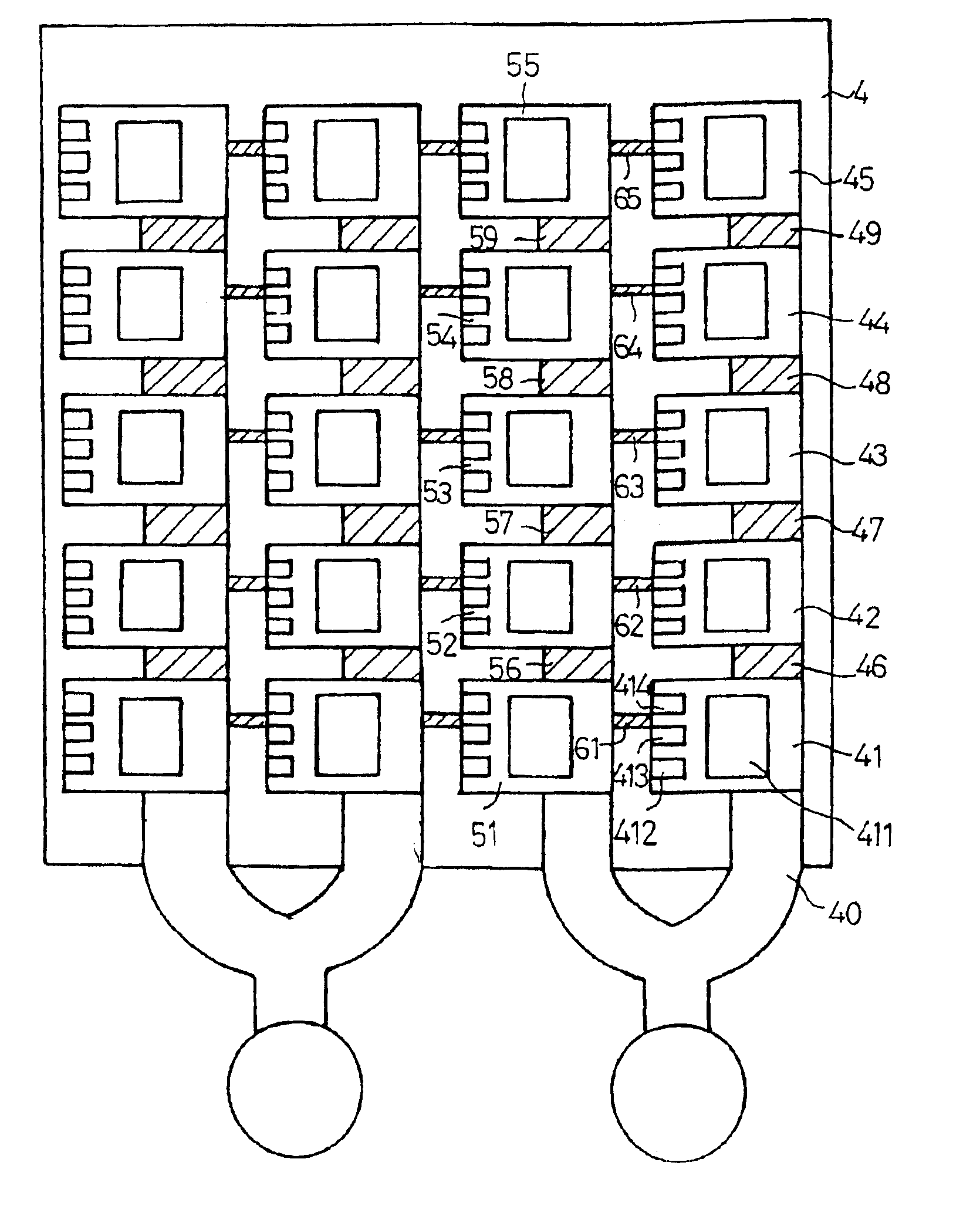
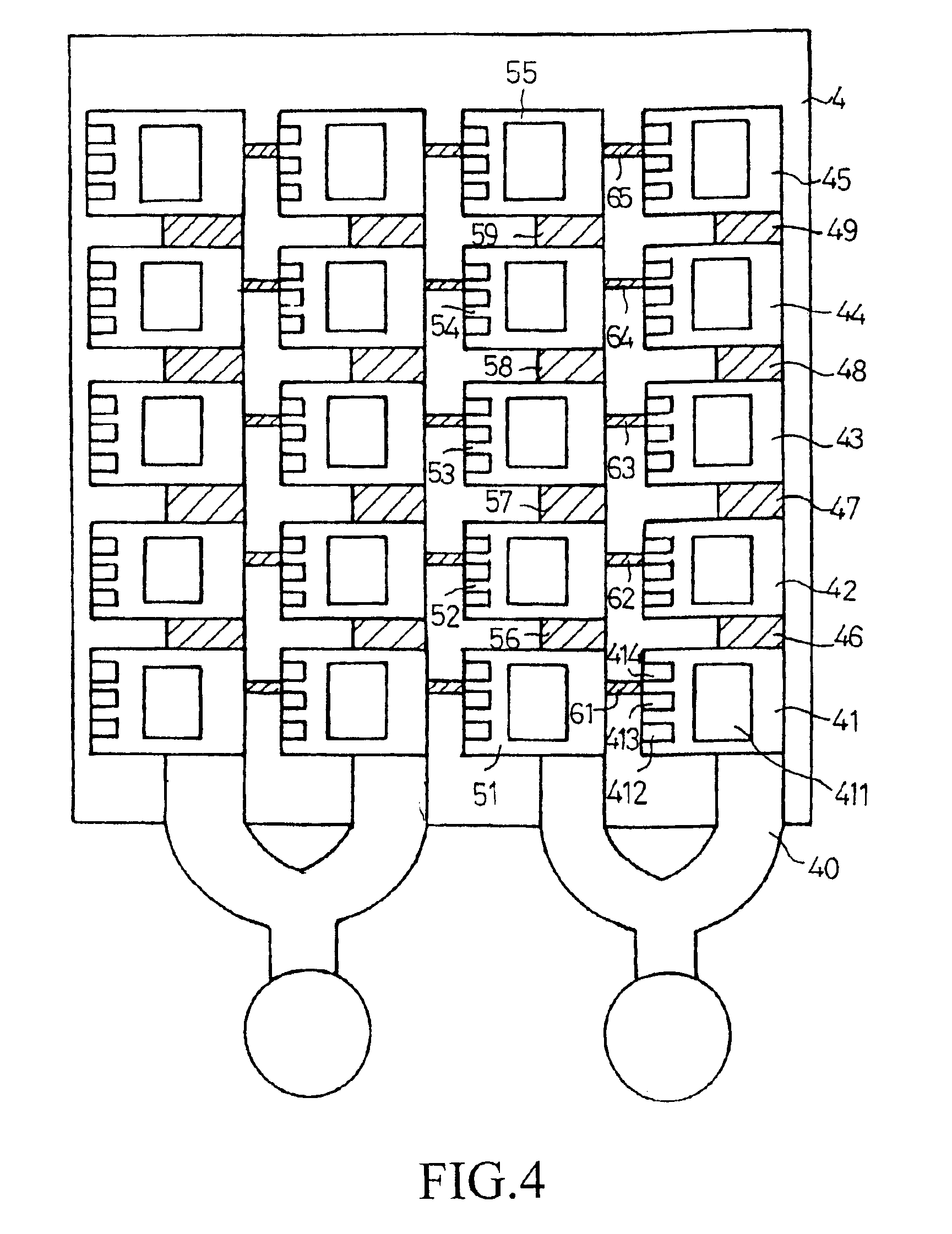
Referring to FIG. 4, according to the invention, a leadframe 4 for leadless semiconductor packages comprises a plurality of cavities 41, 42, 43, 44, 45, 51, 52, 53, 54, 55 and a plurality of inter-cavity longitudinal gates 46, 47, 48, 49, 56, 57, 58, 59. Each cavity has a die pad (not shown in the figure) for supporting a die. Die 411 is, for example, attached to its die pad in cavity 41. Each cavity has a plurality of conducting portions for electrical connection to the die on the die pad. For example, the cavity 41 has three conducting portions 412, 413 and 414. In the embodiment of the invention illustrated in FIG. 4, each cavity has one die pad for supporting a die. To improve the efficiency, each cavity can have a plurality of die pads for supporting a plurality of dice.

The cavities are arranged in a matrix configuration, and are classified into a plurality of columns and a plurality of rows. For example, the cavities 41, 42, 43, 44 and 45 form a first column, and the cavities ...


PUM


Abstract

An encapsulation technique for leadless semiconductor packages entails: (a) attaching a plurality of dice (411) to die pads in cavities (41-45, 51-55) of a leadframe, the cavities arranged in a matrix of columns and rows; (b) electrically connecting the dice to a plurality of conducting portions (412-414) of the leadframe; and (c) longitudinally injecting molding material into the cavities along the columns via a plurality of longitudinal gates (46-49, 56-59) of the leadframe to package the dice in the cavities, the longitudinal gates situated between the cavities along the columns.

Description

BACKGROUND OF THE INVENTION1. Field of the InventionThe present invention relates to an encapsulation method and leadframe for semiconductor packages and, more particularly, to an encapsulation method and leadframe for leadless semiconductor packages.2. Description of the Related ArtConventional encapsulation methods for packaging semiconductor devices are classified into two kinds. The first encapsulation method is applied to semiconductor packages with leads, as shown in FIG. 1. A plurality of dice are respectively mounted in cavities 11 of a leadframe 1, and are connected to the pins of the leadframe 1. The leadframe 1 has runner 12, and the runner 12 is connected to cavities 11 by sub-runners 13 and gates 14. Each gate 14 is an injection inlet between a sub-runner 13 and a cavity 11. Molding material is injected into the runner 12 and moves via the sub-runners 13 and the gates 14 to cavities 11 so as to package the dice in cavities 11. This encapsulation method requires space fo...

Claims


Application Information

Patent Timeline
IPC IPC(8): H01L21/56H01L21/02H01L23/28H01L23/31
CPCH01L21/565H01L2924/0002H01L23/3107H01L2924/00
Inventor KUO, FRANK
Owner SILICONX TAIWAN
Features
  • Generate Ideas
  • Intellectual Property
  • Life Sciences
  • Materials
  • Tech Scout
  • Unparalleled Data Quality
  • Higher Quality Content
  • 60% Fewer Hallucinations
Learn More