Flexible printed circuit substrate

a printed circuit board and flexible technology, applied in the direction of printed circuit aspects, printed circuit manufacturing, semiconductor/solid-state device details, etc., can solve the problems of limited positioning accuracy in the blanking process, inability to precisely connect, and relatively low positioning accuracy achievable by positioning holes and guide pins, so as to improve the productivity of flexible printed circuit boards, the effect of reducing the laser process

Active Publication Date: 2005-02-22
SUMITOMO ELECTRIC PRINTED CIRCUITS INC
View PDF4 Cites 23 Cited by
  • Summary
  • Abstract
  • Description
  • Claims
  • Application Information

AI Technical Summary

Benefits of technology

With such a structure, since the reinforcing film to be processed into the reinforcing board is composed of a resin film with a thickness of 300 μm or less which can be easily etched by a laser process, the time required for processing the reinforcing film simultaneously with the base film, etc., in the laser process can be reduced.
Accordingly, when the flexible printed circuit substrate having such a construction is used, the productivity of the flexible printed circuit board can be improved.

Problems solved by technology

However, since the positioning accuracy achievable in the blanking process is limited, a connection failure may be caused such that the terminals 93 cannot be precisely connected to their respective contacts in the connector when the connecting part C of the flexible printed circuit board is attached to the connector.
However, the positioning accuracy achievable by the positioning holes and the guide pins is relatively low, and the deviation is more than about ±100 μm (±0.1 mm).
However, the accuracy obtained by the positioning method according to Japanese Patent No. 2662477 is limited to about ±70 μm, and further improvement in the positioning accuracy is difficult in the method.
Therefore, the positioning accuracy cannot be improved enough to comply with further reduction in the pitch, and the connection failure which occurs when the connecting part C of the flexible printed circuit board 9a is attached to the connector has become a problem again.

Method used


Image

  • Flexible printed circuit substrate
  • Flexible printed circuit substrate
  • Flexible printed circuit substrate

Examples


Embodiment Construction

An embodiment of the present invention will be described below with reference to the accompanying drawings.

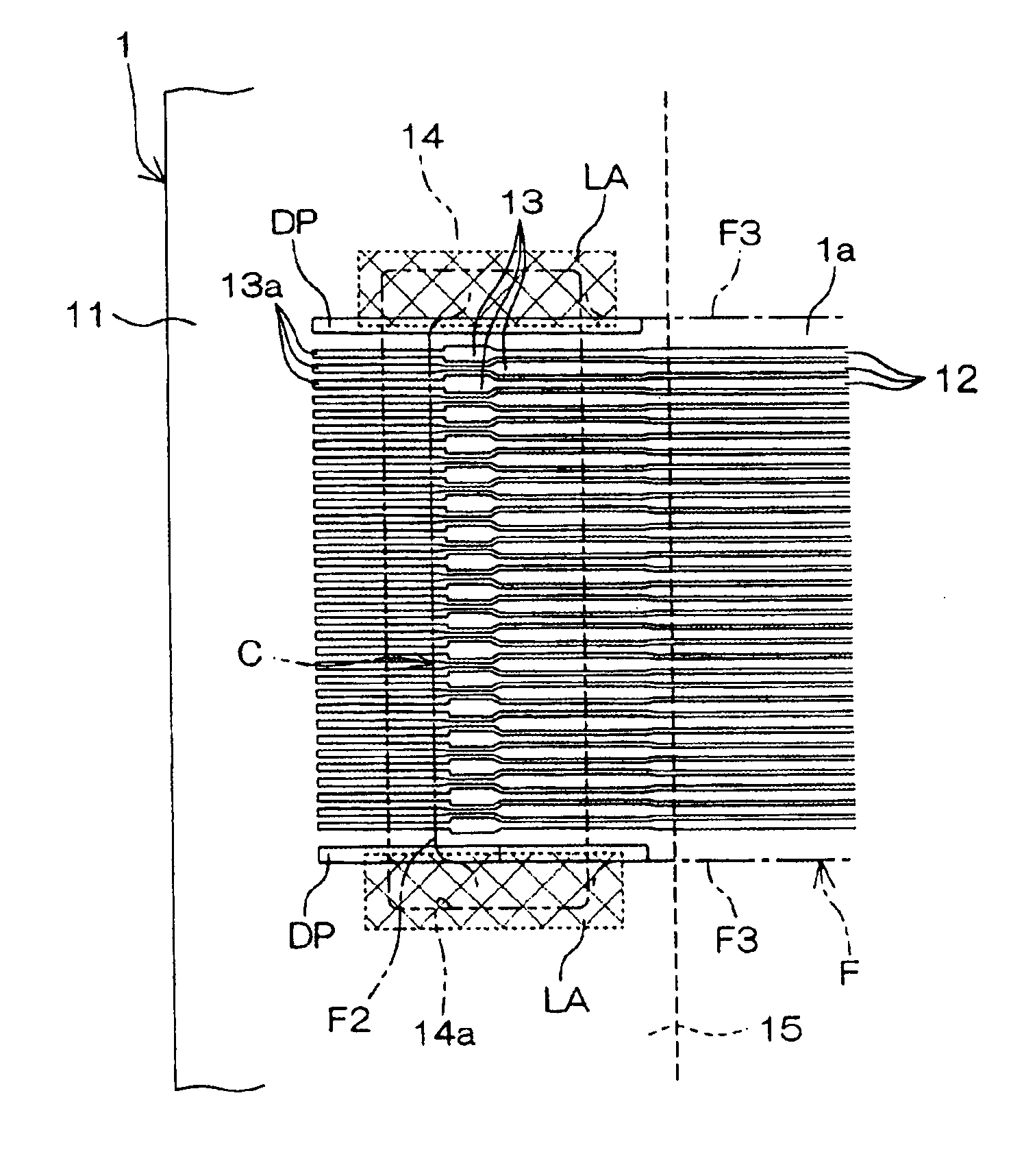
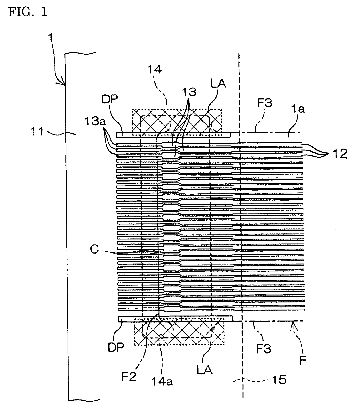
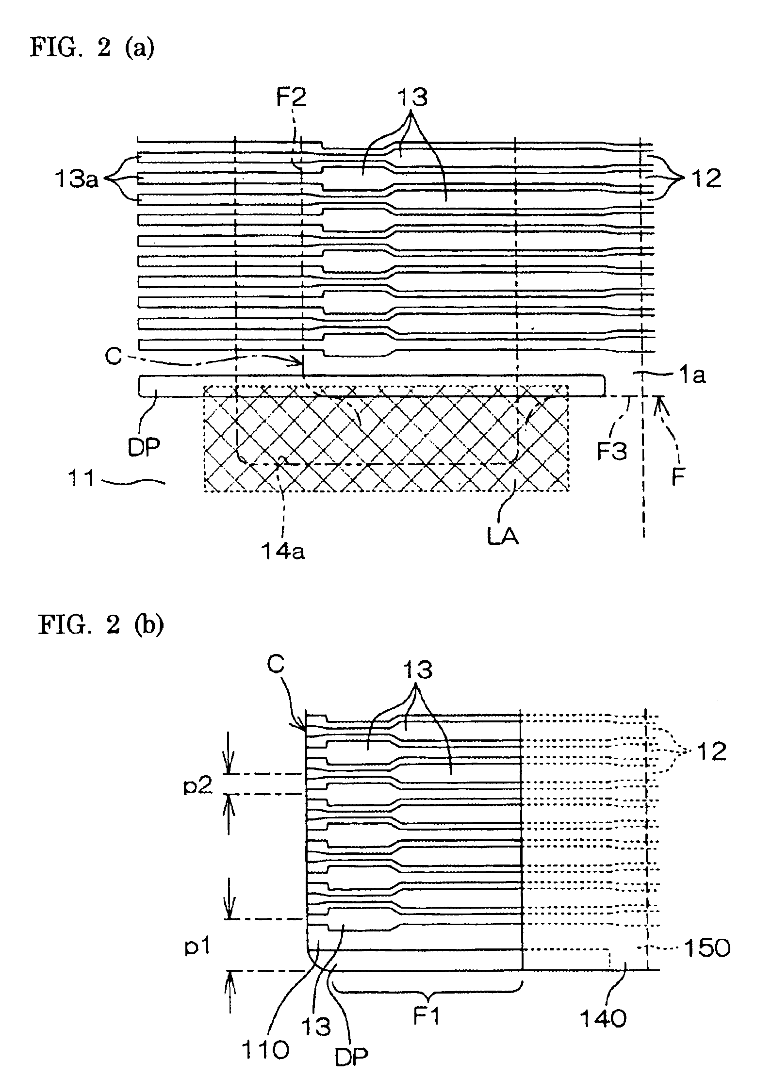
FIG. 1 is an enlarged plan view showing a region around a connecting part C of a flexible printed circuit board 1a in a flexible printed circuit substrate 1 according to an embodiment of the present invention. In addition, FIG. 2(a) is an enlarged plan view showing a region around one of dummy patterns DP used as masks in a laser process for processing a base film 11 in the flexible printed circuit substrate 1.

As shown in the figures, the flexible printed circuit substrate 1 is constructed by forming a region corresponding to the flexible printed circuit board 1a including the connecting part C on the surface of the base film 11 composed of a flexible resin film or the like.

Although only one region corresponding to a single flexible printed circuit board is shown in the figures, two or more regions identical to the above region are normally provided on the surface of a single b...


PUM


Abstract

A novel flexible printed circuit substrate can be processed into a flexible printed circuit board having a high-accuracy connecting part which does not cause a connection failure when it is connected to a connector even if a pitch between two adjacent terminals is further reduced. The flexible printed circuit substrate has dummy patterns which are formed, simultaneously with the terminals, on the sides of the connecting part, in a shape corresponding to the outline of both sides of connecting part which are used for positioning the terminals when the connecting part is attached to the connector. The dummy patterns are used as masks when a base film is subjected to a laser process.

Description

BACKGROUND OF THE INVENTION1. Field of the InventionThe present invention relates to a flexible printed circuit substrate having a connecting part which is to be attached to a connector.2. Description of the Background ArtRecently, electronic devices have become lighter and more compact, and flexible printed circuit boards have come into widespread use as materials for electrical circuits in the electronic devices.A typical flexible printed circuit board has a connecting part which is to be attached to a connector and which is integrally provided on, for example, an edge of the flexible printed circuit board so as to further save space.FIG. 4(a) is an enlarged perspective view of a connecting part C of a flexible printed circuit board 9a. As shown in the figure, the flexible printed circuit board 9a includes a substrate 910 composed of a flexible resin film or the like. The substrate 910 is formed in a predetermined planar shape including the connecting part C which is to be attache...

Claims


Application Information

Patent Timeline
Patent Type & Authority Patents(United States)
IPC IPC(8): H05K3/00H05K1/11H05K3/36H05K1/02
CPCH05K1/118H05K3/0032H05K3/361H05K2201/09145H05K2201/09781H01L2924/0002H05K2203/167H01L2924/00
Inventor KASHIWAGI, SHUJINAGAKUBO, TAKAHIKO
Owner SUMITOMO ELECTRIC PRINTED CIRCUITS INC
Why Eureka
Try Eureka