Lithography using Multilayer Spacer for Reduced Spacer Footing

a multi-layer spacer and spacer technology, applied in the direction of semiconductor/solid-state device manufacturing, basic electric elements, electric devices, etc., can solve the problems of spacers not being substantially spaced, anisotropic etching of spacers may create spacer footings,

Active Publication Date: 2015-04-30
TAIWAN SEMICON MFG CO LTD
View PDF10 Cites 15 Cited by
  • Summary
  • Abstract
  • Description
  • Claims
  • Application Information

AI Technical Summary

Problems solved by technology

However, as semiconductor processes require smaller process windows, the manufacture of these devices have approached and even surpassed the theoretical limits of photolithography equipment.
An issue with this approach is the anisotropic etching of the spacer may create spacer footing due to process limitations for unifor

Method used


Image

  • Lithography using Multilayer Spacer for Reduced Spacer Footing
  • Lithography using Multilayer Spacer for Reduced Spacer Footing
  • Lithography using Multilayer Spacer for Reduced Spacer Footing

Examples


Embodiment Construction

[0006]The making and using of the present embodiments are discussed in detail below. It should be appreciated, however, that the present disclosure provides many applicable inventive concepts that can be embodied in a wide variety of specific contexts. The specific embodiments discussed are merely illustrative of specific ways to make and use the disclosed subject matter, and do not limit the scope of the different embodiments.

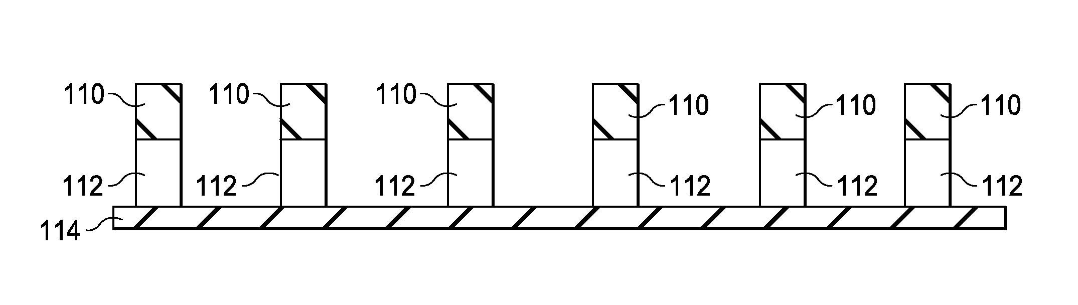
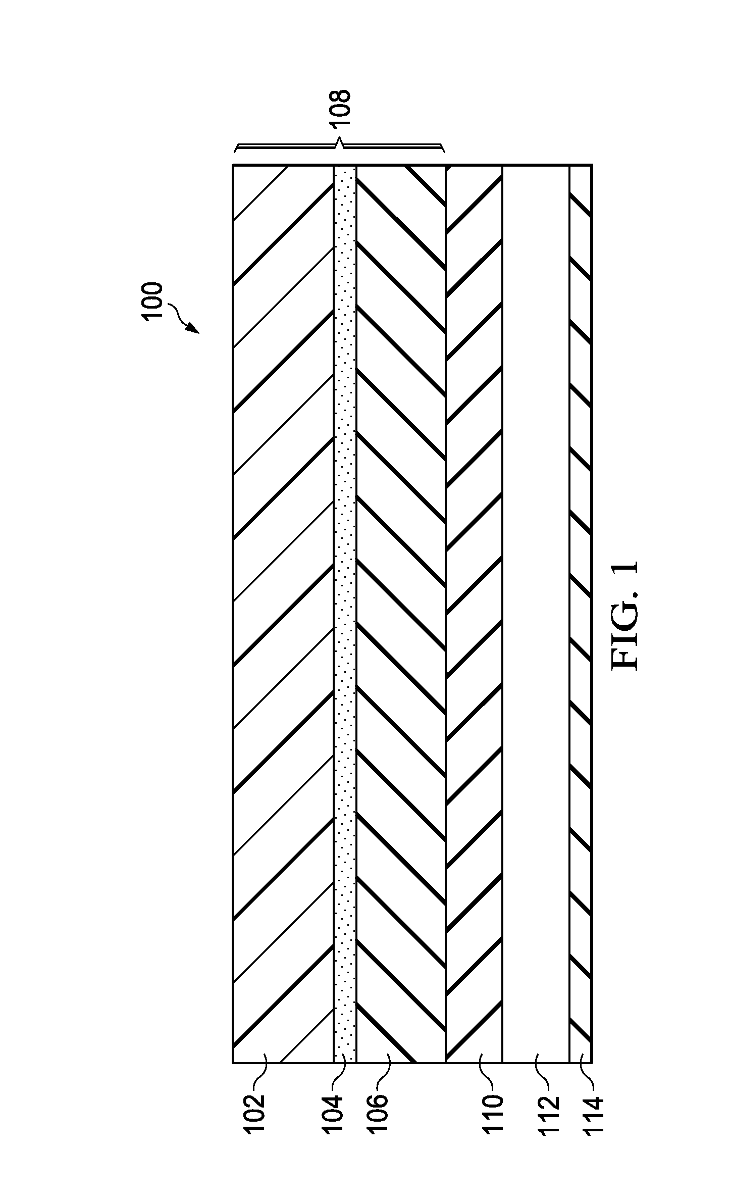
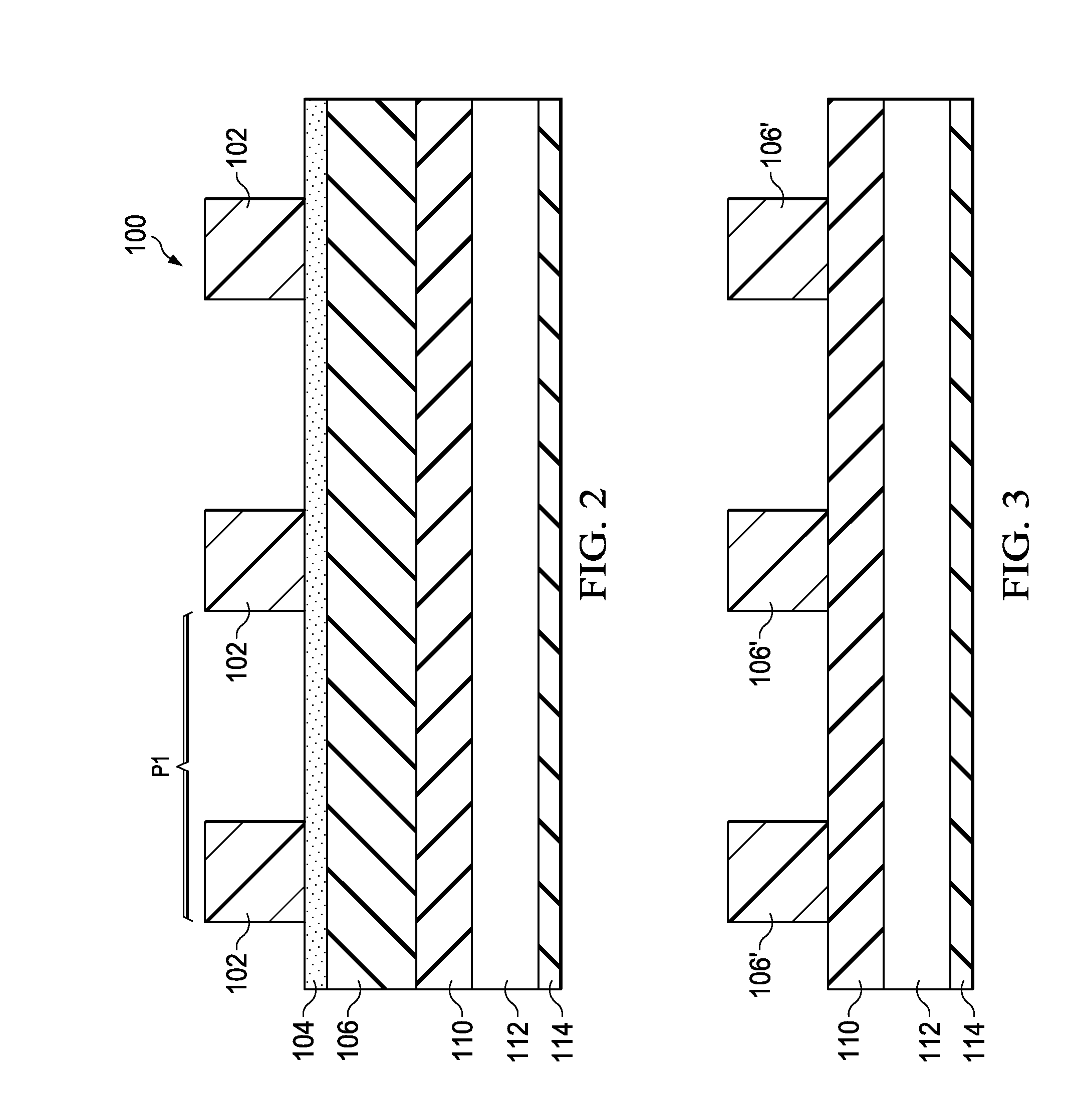
[0007]Various embodiments use a multilayer spacer in a multiple pattern photolithography process to reduce spacer footing and improve process reliability. A plurality of mandrels on a substrate and a multilayer sidewall aligned spacer is conformably formed over the mandrels. The multilayer spacer may be formed by conformably depositing one or more spacer layers over the mandrels and plasma treating each spacer layer after each deposition. The plasma treatment causes the spacer layers to become more compact (i.e., thinner) and easier to etch. The multilayer spa...


PUM


Abstract

A method embodiment for patterning a semiconductor device includes forming a plurality of mandrels over a substrate, and forming a multilayer spacer layer over the plurality of mandrels. The multilayer spacer layer is formed by conformably depositing a spacer layer over the plurality of mandrels and treating the spacer layer with plasma. The plurality of mandrels is exposed by etching a top portion of the multilayer spacer layer, thereby forming a multilayer spacer.

Description

BACKGROUND[0001]With the increasing down-scaling of semiconductor devices, various processing techniques, such as, photolithography are adapted to allow for the manufacture of devices with increasingly smaller dimensions. However, as semiconductor processes require smaller process windows, the manufacture of these devices have approached and even surpassed the theoretical limits of photolithography equipment. As semiconductor devices continue to shrink, the spacing desired between elements (i.e., the pitch) of a device is less than the pitch that can be manufactured using traditional optical masks and photolithography equipment.[0002]One approach used to achieve the higher resolutions to manufacture smaller devices is to use multiple pattern lithography. For example, a half pitch (i.e., half of the minimum photolithographic pitch achievable in a traditional photolithography system) can be achieved by forming mandrels (e.g., at a minimum available pitch), conformably forming a sidewa...

Claims


Application Information

Patent Timeline
IPC IPC(8): H01L21/311H01L21/033H01L21/02H01L21/027
CPCH01L21/31111H01L21/0276H01L21/0234H01L21/02186H01L21/0332H01L21/31116H01L21/0337H01L21/3065H01L21/3105H01L21/31133H01L21/321H01L21/32136
Inventor PENG, CHAO-HSIENLEE, HSIANG-HUANSHUE, SHAU-LIN
Owner TAIWAN SEMICON MFG CO LTD
Why Eureka
Try Eureka