Method for fabricating strained-silicon CMOS transistor

a technology of strained silicon and cmos, which is applied in the direction of electrical transducers, semiconductor devices, transducer details, etc., can solve the problems of affecting the yield of fabricating contact holes in the later process, and the defect of the device, so as to achieve the effect of easy control of the magnitude of the etching process

Active Publication Date: 2008-08-14
UNITED MICROELECTRONICS CORP
View PDF9 Cites 16 Cited by
  • Summary
  • Abstract
  • Description
  • Claims
  • Application Information

AI Technical Summary

Benefits of technology

[0017]A method for fabricating a strained-silicon CMOS transistor is disclosed. The method includes: providing a substrate having a first active region for fabricating a first transistor, a second active region for fabricating a second transistor, and an isolation structure disposed between the first active region and the second active region; forming a gate structure on the first active region and a second gate structure on the second active region; forming a source / drain region for the first transistor and a source / drain region for the second transistor; forming a first etching stop layer, a first stress layer, and a second etching stop layer on the first transistor, the second transistor, and the isolation structure; forming a first patterned photoresist on the second etching stop layer of the first active region; performing a first etching process to remove the second etching stop layer and a portion of the first stress layer of the second active region; removing the first patterned photoresist; and performing a second etching process by utilizing the second etching stop layer of the first active region as a mask to remove the remaining first stress layer of the second active region. Thereafter, a second stress layer is formed on the first etching stop layer of the second active region, in which a gap is formed between the first stress layer and the second stress layer. This completes the fabrication of a strained-silicon CMOS transistor.
[0019]Preferably, the present invention forms a first etching stop layer, a stress layer, and a second etching stop layer on a first transistor and a second transistor, disposes a patterned photoresist on the first transistor, and uses the patterned photoresist as a mask to remove the second etching stop layer and a portion of the stress layer from the second transistor. After removing the patterned photoresist, the second etching stop layer on the first transistor is used as a mask to remove the remaining stress layer on the second transistor. In other words, in contrast to the conventional method of using a single step etching method, the present invention proposes a two-step etching process to remove a stress layer from a transistor, in which the magnitude of the etching process can be easily controlled. By using the two-step etching process, the problem of over-etching the salicide layer formed on the surface of the substrate can be prevented.
[0020]According to another embodiment of the present invention, the region connecting the high tensile stress film and the high compressive stress film is also removed during the process for fabricating a dual contact etch stop layer. By forming a gap between the two stress layers, phenomenon such as peeling as a result of staking one stress layer on top of another can be prevented.

Problems solved by technology

This method removes the stress layer from the transistor rapidly, but also over-etches and damages the salicide layer disposed under the stress layer and ultimately influences the yield for fabricating contact holes in the later process.
Additionally, during the process for etching the high tensile stress film disposed on the NMOS transistor and the high compressive stress film disposed on the PMOS transistor, the definition of the region between the two stress layers is difficult and easily result in an overlapping phenomenon, as shown in FIG. 5, in which one stress layer is stacked on top of another.
If the width of the overlapping region of the two stress layers is greater than 30 nm, the peeling phenomenon is prevented but after a series of back end processes such as photoresist stripping or chemical mechanical polishing are performed, the overlapping region would break and result in defect of the device.

Method used


Image

  • Method for fabricating strained-silicon CMOS transistor
  • Method for fabricating strained-silicon CMOS transistor
  • Method for fabricating strained-silicon CMOS transistor

Examples


Embodiment Construction

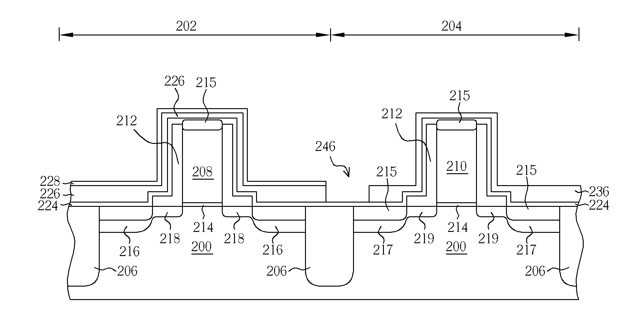
[0025]Please refer to FIGS. 7-13. FIGS. 7-13 are perspective diagrams illustrating a method for fabricating dual contact etch stop layer on a strained-silicon CMOS transistor according to the present invention. As shown in FIG. 7, a semiconductor substrate 200 having an NMOS region 202 and a PMOS region 204 is provided, in which the NMOS region 202 and the PMOS region 204 are divided by a shallow trench isolation 206. Each of the NMOS region 202 and the PMOS region 204 includes a gate structure. The NMOS gate structure includes an NMOS gate 208 and a gate dielectric 214 disposed between the NMOS gate 208 and the semiconductor substrate 200. The PMOS gate structure includes a PMOS gate 210 and a gate dielectric 214 disposed between the PMOS gate 210 and the semiconductor substrate 200. The sidewall of the NMOS gate 208 and the PMOS gate 210 includes a liner 212 composed of silicon dioxide or silicon nitride.

[0026]Next, an ion implantation process is performed to form a source / drain r...


PUM


Abstract

First, a semiconductor substrate having a first active region and a second active region is provided. The first active region includes a first transistor and the second active region includes a second transistor. A first etching stop layer, a stress layer, and a second etching stop layer are disposed on the first transistor, the second transistor and the isolation structure. A first etching process is performed by using a patterned photoresist disposed on the first active region as a mask to remove the second etching stop layer and a portion of the stress layer from the second active region. The patterned photoresist is removed, and a second etching process is performed by using the second etching stop layer of the first active region as a mask to remove the remaining stress layer and a portion of the first etching stop layer from the second active region.

Description

BACKGROUND OF THE INVENTION [0001]1. Field of the Invention[0002]The invention relates to a method for fabricating a strained-silicon CMOS transistor.[0003]2. Description of the Prior Art[0004]As semiconductor technology advances and development of integrated circuits continues to revolution, the computing power and storage capacity enjoyed by computers also increases exponentially. As a result, this growth further fuels the expansion of related industries. As predicted by Moores Law, the number of transistors utilized in integrated circuits has doubled every 18 months and semiconductor processes also have advanced from 0.18 micron in 1999, 0.13 micron in 2001, 90 nanometer (0.09 micron) in 2003, to 65 nanometer (0.065 micron) in 2005.[0005]As the semiconductor processes advance, determining methods for increasing the driving current for metal oxide semiconductor (MOS) transistors for fabrication processes under 65 nanometers has become an important topic. Currently, the utilization...

Claims


Application Information

Patent Timeline
Patent Type & Authority Applications(United States)
IPC IPC(8): H01L27/092H01L21/8238
CPCH01L29/7843H01L21/823807
Inventor CHOU, PEI-YUTZOU, SHIH-FANGLIAO, JIUNN-HSIUNG
Owner UNITED MICROELECTRONICS CORP
Why Eureka
Try Eureka