Semiconductor device with pillar-shaped capacitor storage node and method of fabricating the same

a technology of capacitor storage node and semiconductor device, which is applied in the direction of semiconductor device, capacitor, electrical apparatus, etc., can solve the problems of difficult metal interconnection, increased leakage current of high dielectric film, and use of platinum in highly integrated circuit devi

Inactive Publication Date: 2001-04-17
SAMSUNG ELECTRONICS CO LTD
View PDF11 Cites 17 Cited by
  • Summary
  • Abstract
  • Description
  • Claims
  • Application Information

AI Technical Summary

Problems solved by technology

The increase in the height of the capacitor at the cell array region, however, causes a large step between the cell array region and peripheral region, thus making it difficult to form metal interconnections.
However, when the polysilicon is used as a capacitor storage node, a layer of low dielectric characteristics, such as SiO.sub.2 (silicon oxide layer) is formed at the interface between the polysilicon layer and the high dielectric film, thereby increasing the leakage current of the high diel

Method used


Image

  • Semiconductor device with pillar-shaped capacitor storage node and method of fabricating the same
  • Semiconductor device with pillar-shaped capacitor storage node and method of fabricating the same
  • Semiconductor device with pillar-shaped capacitor storage node and method of fabricating the same

Examples


Embodiment Construction

Korean Patent Application No. 98-26916, filed on Jul. 3, 1998, is hereby incorporated by reference in its entirety as if fully set forth herein.

The present invention will now be described more fully hereinafter with reference to the accompanying drawings, in which preferred embodiments of the invention are shown. This invention may, however, be embodied in different forms and should not be construed as limited to the embodiments set forth herein. Rather, these embodiments are provided so that this disclosure will be thorough and complete, and will fully convey the scope of the invention to those skilled in the art.

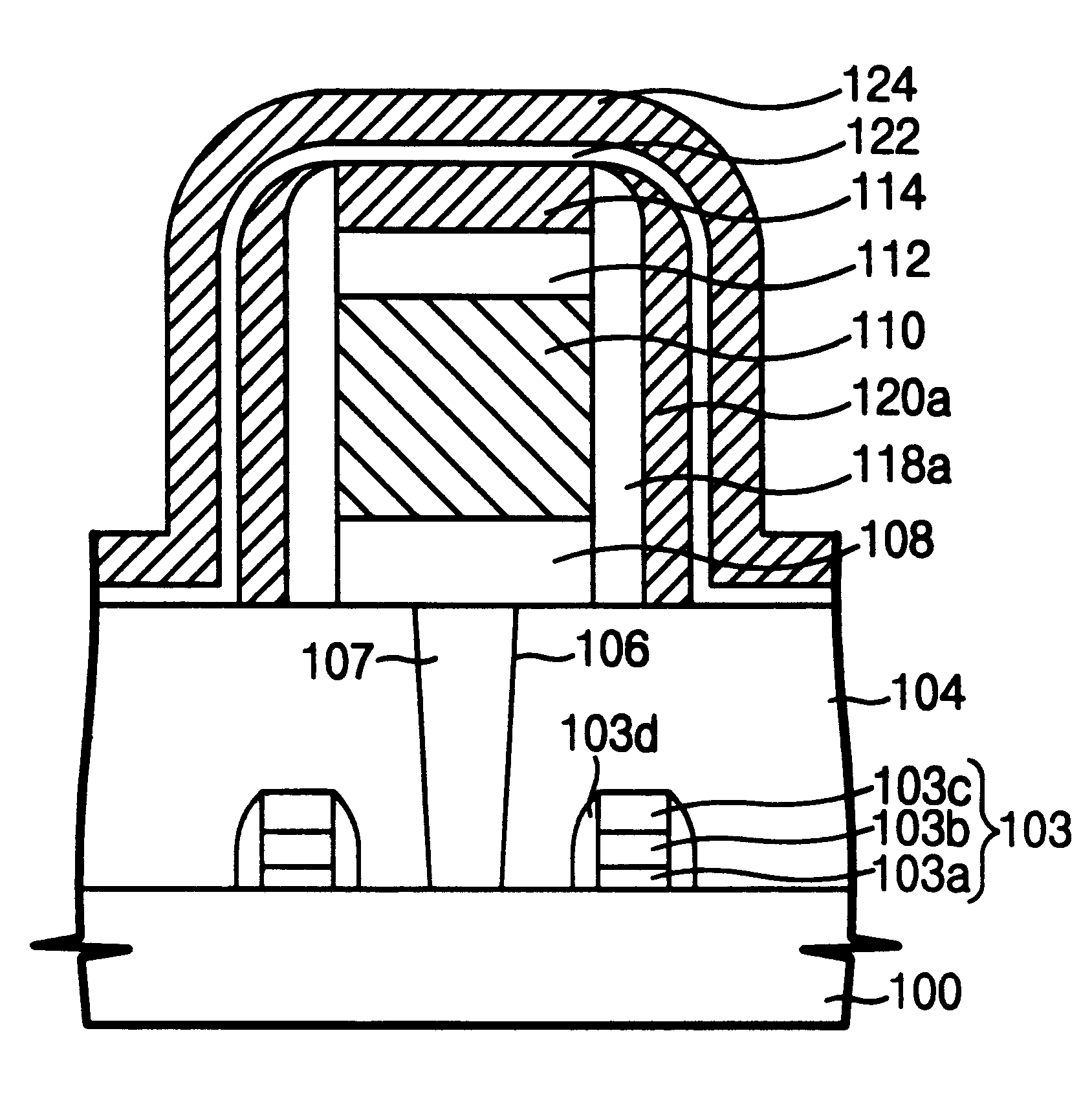
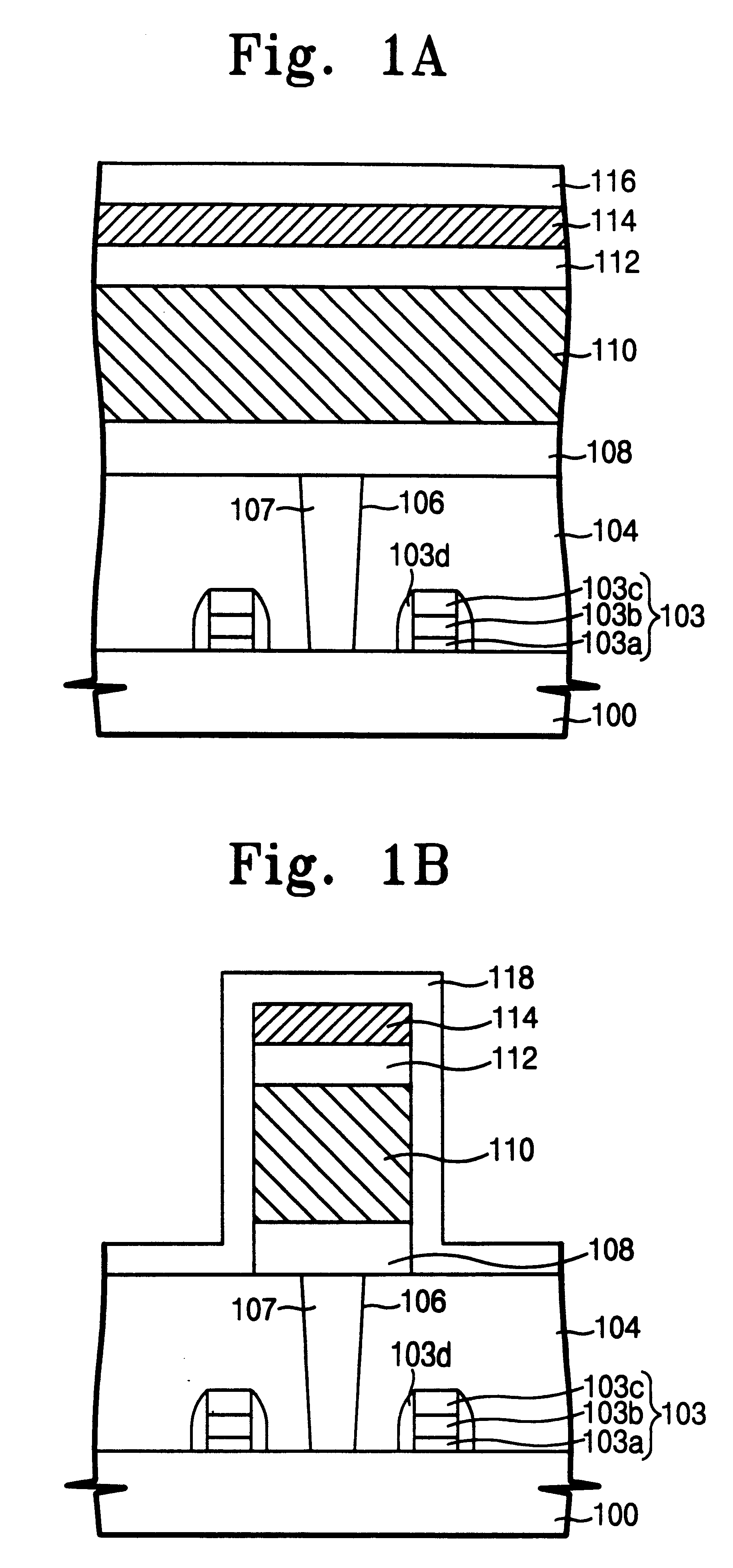
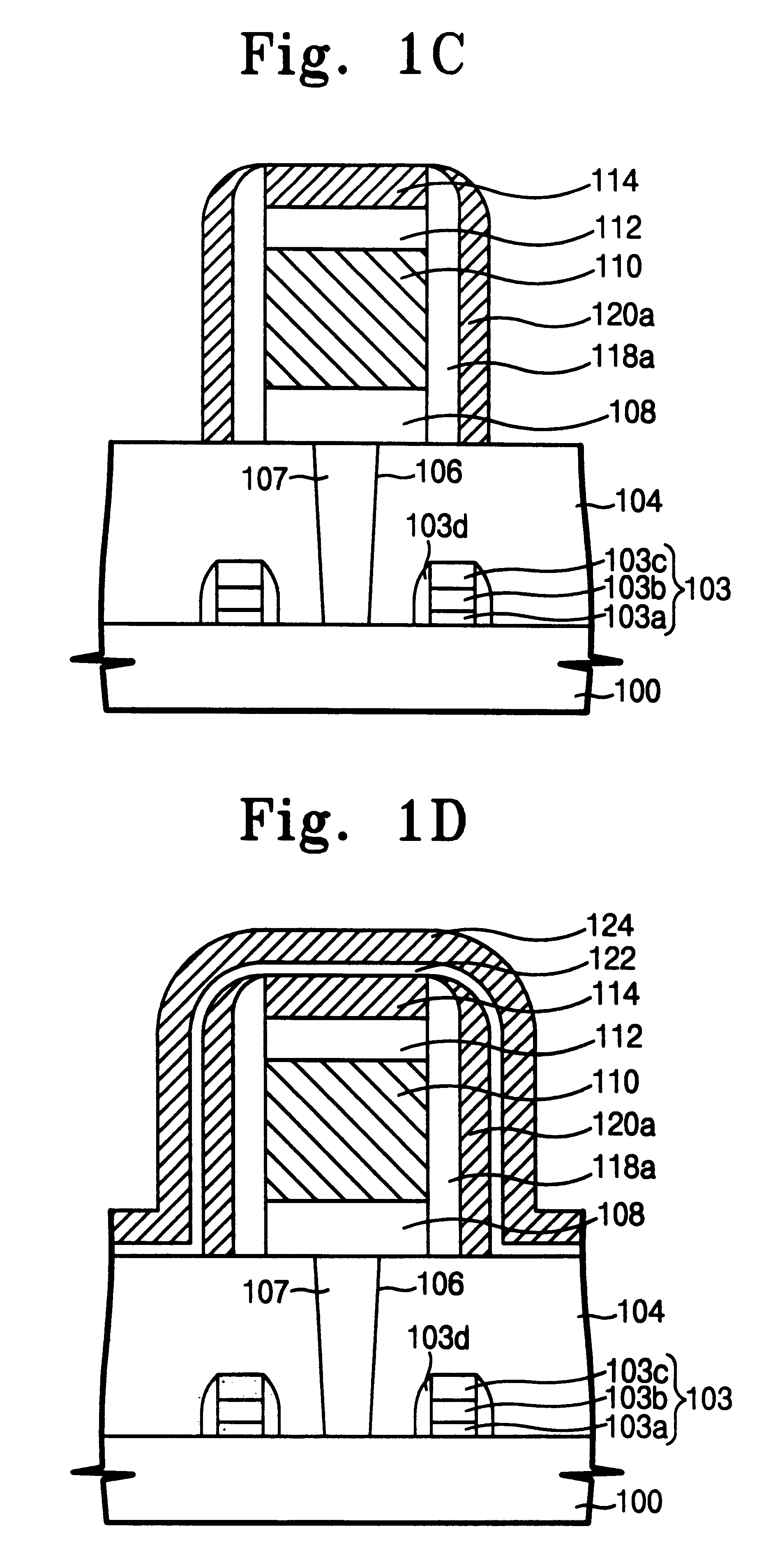
In the drawings, the thickness of layers and regions are exaggerated for clarity. It will also be understood that when a layer is referred to as being "on" another layer or substrate, it can be directly on the other layer or substrate or intervening layers may also be present. In contrast, when an element is referred to as being "directly on" another element, there are no ...


PUM


Abstract

A semiconductor device and a method for making a semiconductor device having a pillar-shaped capacitor storage node compatible with a high dielectric film, wherein the pillar-shaped capacitor storage node includes a thick conductive metal layer that is easily etched and a thin conductive layer completely coating the thick conductive metal layer. The thin conductive layer protects the thick conductive metal layer during subsequent high dielectric deposition and annealing and various oxidation process.

Description

1. Field of the InventionThe present invention relates to a semiconductor device and a method of manufacturing such a device. More particularly, the present invention relates to a semiconductor device having a pillar-shaped capacitor storage node having a high dielectric film and a method for manufacturing such a device.2. Background of the InventionConventional dynamic random access memory (DRAM) devices include storage nodes, which storage nodes typically include a capacitor. As DRAM devices are scaled down to a line width dimension of about a quarter micrometer, two-dimensional areas occupied by the capacitor become smaller and smaller. Despite reduced cell areas, capacitors require a minimum level of capacitance of about 25 fF to 30 fF. Many methods have therefore been developed to maintain a desired capacitance from decreased two-dimensional areas.One approach is to increase the height of the capacitor so as to increase the available cell surface areas. The increase in the heig...

Claims


Application Information

Patent Timeline
IPC IPC(8): H01L21/02H01L21/70H01L21/8242H01L27/108
CPCH01L27/10852H01L28/82H01L28/90H10B12/033H10B12/00
Inventor KWAK, DONG-HWAHWANG, YOO-SANGCHUNG, TAE-YOUNG
Owner SAMSUNG ELECTRONICS CO LTD
Why Eureka
Try Eureka