Thermoelectric conversion element and producing method thereof

a technology of thermoelectric elements and conversion elements, which is applied in the manufacture/treatment of thermoelectric devices, thermoelectric devices with peltier/seeback effects, electrical apparatus, etc., can solve the problems of degrading the yield of thermoelectric materials, chip breaking during cutting, and significant deformation of yield, so as to reduce stress applied to each thermoelectric material layer, reduce the number of pn junction pairs per unit area, and suppress the breakage of thermoelectric material chips

Inactive Publication Date: 2013-10-31
PANASONIC INTELLECTUAL PROPERTY MANAGEMENT CO LTD
View PDF1 Cites 16 Cited by
  • Summary
  • Abstract
  • Description
  • Claims
  • Application Information

AI Technical Summary

Benefits of technology

[0049]In the invention, the thermoelectric conversion element comprises the alternate layers of the p-type thermoelectric material layers and the n-type thermoelectric material layers, and the plurality of substrates disposed between adjacent layers of the p-type thermoelectric material layers and n-type thermoelectric material layers. Therefore, the number of pn junction pairs per unit area can be increased, and the breakage of the thermoelectric material chip can be suppressed.
[0050]In the invention, the contact holes are alternately disposed at opposite ends of the substrates in the direction perpendicular to the direction of arrangement of the p-type thermoelectric material layers and the n-type thermoelectric material layers, and the conductive material is disposed in the contact holes. The stress applied to each thermoelectric material layer is reduced, because each thermoelectric material layer and the conductive material come easily and securely into contact with each other when the substrates are stacked. Therefore, the substrate and each thermoelectric material layer can be formed thinner. Accordingly, the number of pn junction pairs per unit area can be increased.
[0051]In the thermoelectric conversion element of the invention,the plurality of substrates are disposed between adjacent layers of the p-type thermoelectric material layers and n-type thermoelectric material layers, and the contact holes are disposed alternately at opposite ends of the substrates. Therefore, productivity is enhanced in the thermoelectric conversion element of the invention compared with the case in which the p-type thermoelectric material layer and the n-type thermoelectric material layer, which are alternately stacked with the substrate interposed therebetween, are connected by the electrode formed at the edge like the conventional thermoelectric conversion element.
[0052]According to the thermoelectric conversion element of the invention, the number of pn junction pairs per unit area is increased because the p-type thermoelectric material layers and the n-type thermoelectric material layers are formed into a layered shape. Therefore, the high output can be obtained. Because the plurality of substrates are disposed between adjacent layers of the p-type thermoelectric material layers and n-type thermoelectric material layers, reliability degradation caused by the breakage of the thermoelectric material can be prevented irrespective of the thermoelectric material.

Problems solved by technology

Therefore, when the thermoelectric conversion element is subjected to processes such as slicing and dicing in order to obtain the thermoelectric conversion element from an ingot, a yield may be significantly degraded due to a crack and a chip.
However, because a wafer is cut and removed to prepare the thermoelectric material chip whose section is small in a surface which is parallel to the substrate of the thermoelectric material chip, the conventional configuration has a problem in that the chip is broken during the cutting and removing process and during use.
Additionally, the thermoelectric material chip is prepared by cutting and removing the wafer, which results in another problem in that the yield of the thermoelectric material is degraded.

Method used


Image

  • Thermoelectric conversion element and producing method thereof
  • Thermoelectric conversion element and producing method thereof
  • Thermoelectric conversion element and producing method thereof

Examples


embodiment 1

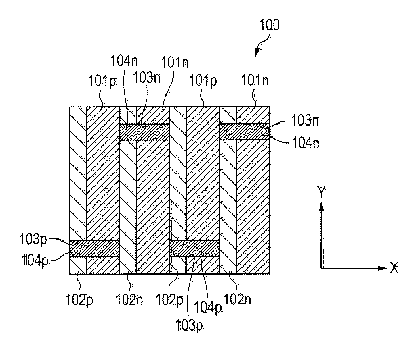
[0063]FIG. 1 is a view illustrating a schematic configuration of thermoelectric conversion element 100 according to Embodiment 1 of the invention. FIG. 1(a) is a perspective view, and FIG. 1(b) is a sectional view taken on a line A-A of FIG. 1(a).

[0064]As illustrated in FIG. 1, thermoelectric conversion element 100 of Embodiment 1 includes plural substrates 101, and alternate layers of p-type thermoelectric material layer 102p and n-type thermoelectric material layer 102n. The plurality of substrates 101 are disposed between adjacent layers of p-type thermoelectric material layer 102p and n-type thermoelectric material layer 102n. The plurality of substrates 101 have contact holes 103 such that contact holes 103 are disposed alternately at opposite ends, in the direction perpendicular to the direction of arrangement of p-type thermoelectric material layer 102p and n-type thermoelectric material layer 102n, of substrates 101. In FIG. 1, the sign X designates the direction of arrangem...

embodiment 2

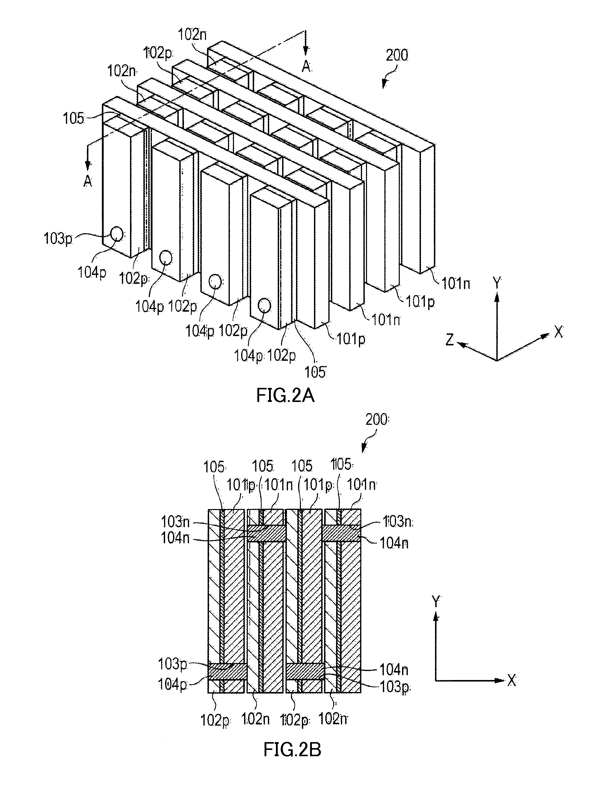
[0089]FIG. 2 is a view illustrating a schematic configuration of thermoelectric conversion element 200 according to Embodiment 2 of the invention. FIG. 2(a) is a perspective view, and FIG. 2(b) is a sectional view taken on a line A-A of FIG. 2(a).

[0090]As illustrated in FIG. 2, plural substrates 101p and plural substrates 101n are alternately disposed in thermoelectric conversion element 200 of Embodiment 2. P-type thermoelectric material layer 102p is formed in the surface of each of substrates 101p, and n-type thermoelectric material layer 102n is formed in the surface of each of substrates 101n. Plural segments of p-type thermoelectric material layer 102p are formed in one substrate 101p. Plural segments of n-type thermoelectric material layer 102n are formed in one substrate 101n. As illustrated in FIG. 2(a), p-type thermoelectric material layers 102p and n-type thermoelectric material layers 102n are respectively arrayed in the Z-direction on each substrate 101. Each segments o...

embodiment 3

[0118]In the thermoelectric conversion element of the invention, the p-type thermoelectric material layers and the n-type thermoelectric material layers are alternately disposed along the X-direction, the disposition of the contact hole may vary in the Y-direction, and the disposition of the thermoelectric material layer may vary in the Z-direction on the same substrate.

[0119]For example, in thermoelectric conversion element 300 illustrated in FIG. 5, p-type thermoelectric material layers 102p and n-type thermoelectric material layers 102n are alternately arrayed along the X-direction. On one substrate 101′, segments of p-type thermoelectric material layers 102p and segments of n-type thermoelectric material layers 102n are alternately disposed along the Z-direction, respectively. For example: a segment of p-type thermoelectric material layer 102p that includes contact hole 103p on one end side in the Y-direction; a segment of n-type thermoelectric material layer 102n that includes ...


PUM


Abstract

The invention provides a thermoelectric conversion element having a lot of pn junction pairs per unit area and having a thermoelectric material chip which is hardly broken, and a producing method thereof. In the thermoelectric conversion element of the invention, plural substrates in each of which a film-shaped thermoelectric material is formed in a surface thereof are disposed. As a result, because the number of pn junction pairs per unit area is increased, a high output can be obtained. Because the thermoelectric material is formed into the film shape, reliability degradation caused by a breakage of the thermoelectric material can be prevented, even in the thermoelectric material having many pn junction pairs per unit area, namely, a sectional area is small.

Description

TECHNICAL FIELD[0001]The present invention relates to a thermoelectric conversion element and a producing method thereof.BACKGROUND ART[0002]An element in which a Peltier effect or a Seebeck effect is utilized is used as a thermoelectric conversion element. The thermoelectric conversion element has a simple structure, and the thermoelectric conversion element is easily handled to be able to maintain a stable characteristic. Therefore, the thermoelectric conversion element attracts attention of a wide variety of applications. Particularly, because the thermoelectric conversion element can perform to cool a limited part and to control a temperature of the limited part near room temperature, accurately, as an electronic cooling element, researches are widely conducted toward applications of optoelectronics and a an isothermal treatment of a semiconductor laser.[0003]Conventionally, as illustrated in FIG. 8, in configuration of the thermoelectric conversion element used in electronic co...

Claims


Application Information

Patent Timeline
Patent Type & Authority Applications(United States)
IPC IPC(8): H01L35/04H01L35/34
CPCH01L35/04H01L35/34H10N10/81H10N10/852H10N10/17H10N10/01
Inventor TOYODA, KAORIHIGASHIDA, TAKAAKIOHIDO, YOSHIHISAKUBO, TAKASHI
Owner PANASONIC INTELLECTUAL PROPERTY MANAGEMENT CO LTD
Why Eureka
Try Eureka