

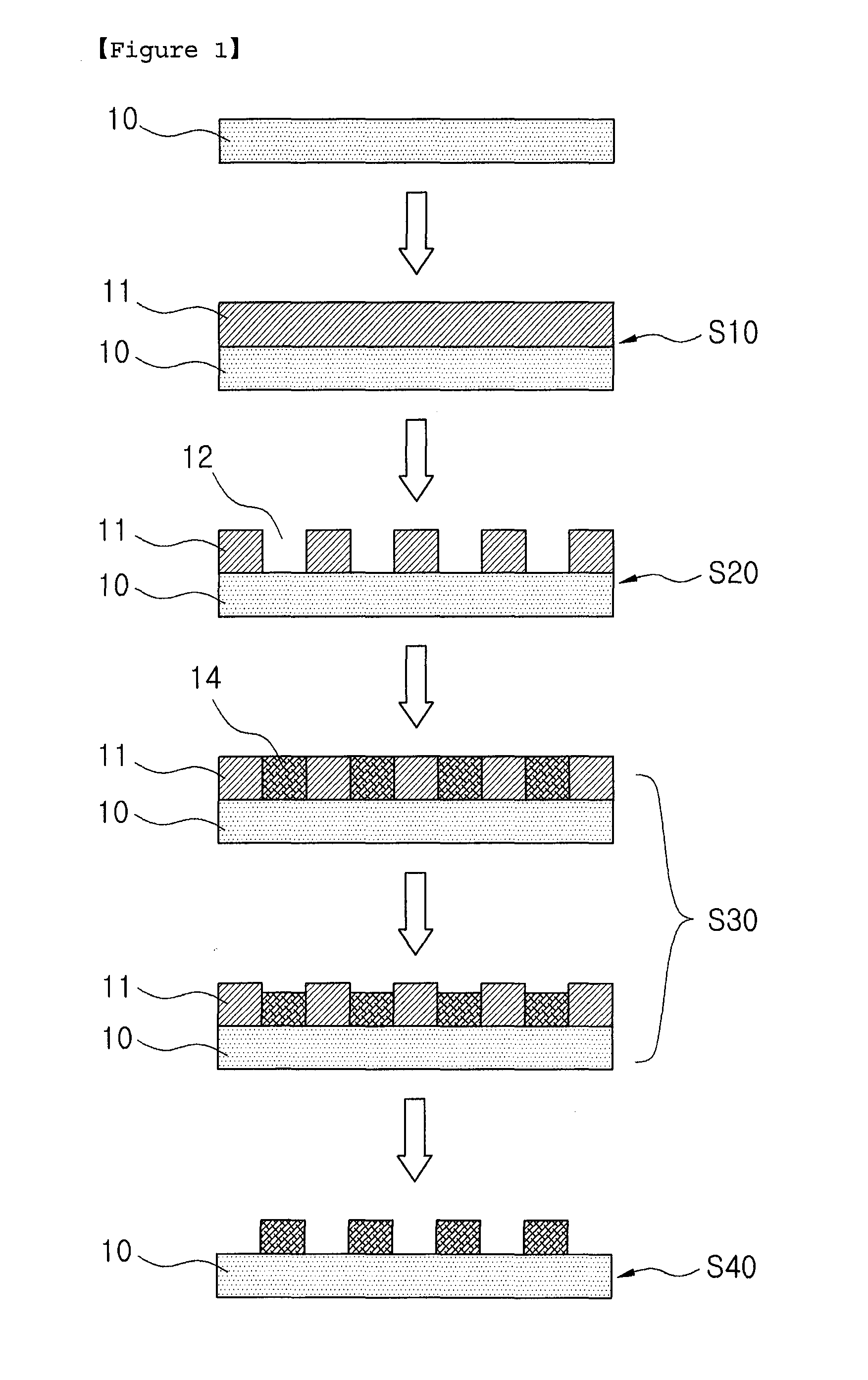
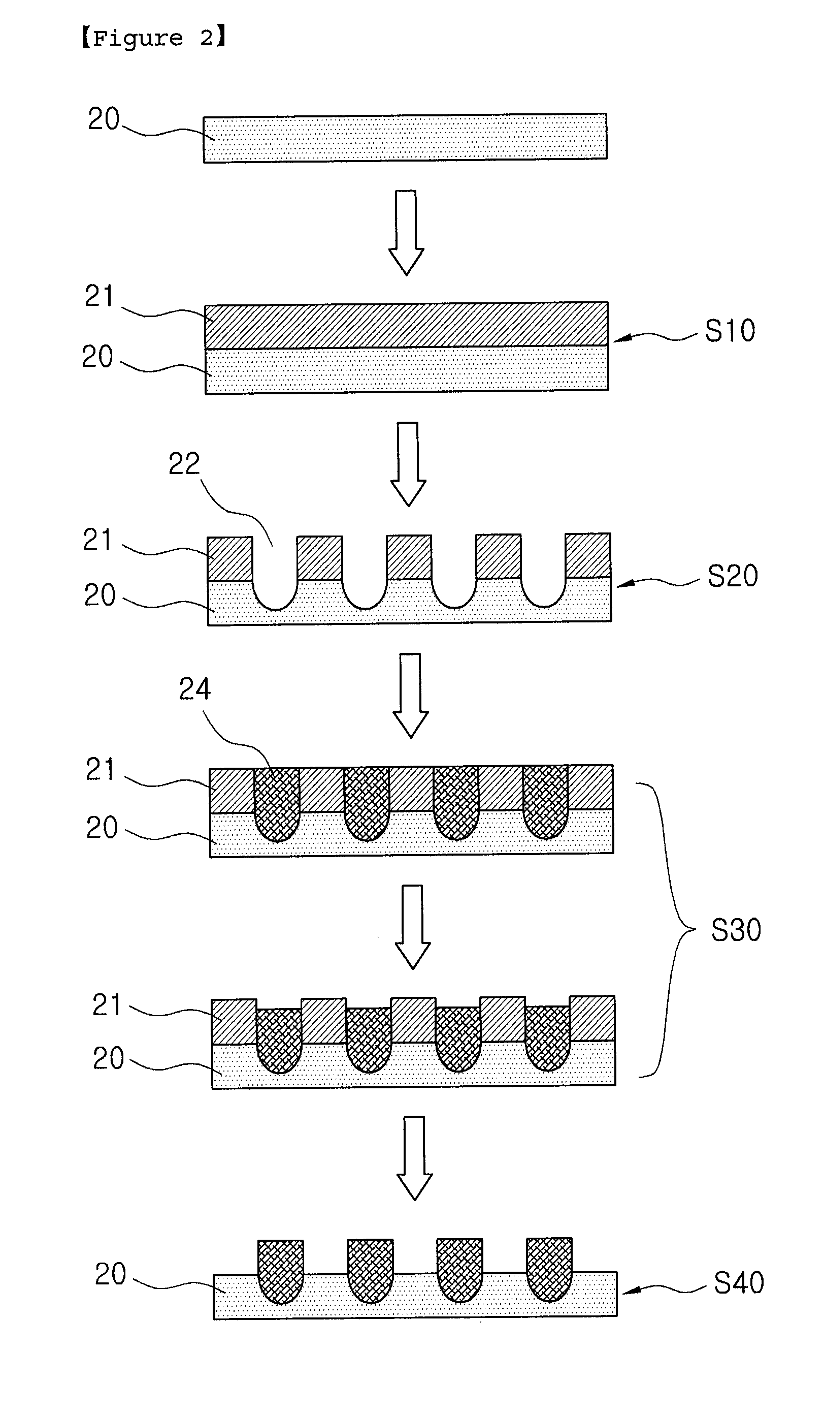
Method for Fabricating Blackened Conductive Patterns
a technology of blackened conductive patterns and fabrication methods, applied in the direction of dielectric characteristics, liquid/solution decomposition chemical coating, light absorption dielectrics, etc., can solve the problems of high cost, large sized equipment required according to the etching, and complex fabrication process
- Summary
- Abstract
- Description
- Claims
- Application Information
AI Technical Summary
Benefits of technology
Problems solved by technology
Method used
Image

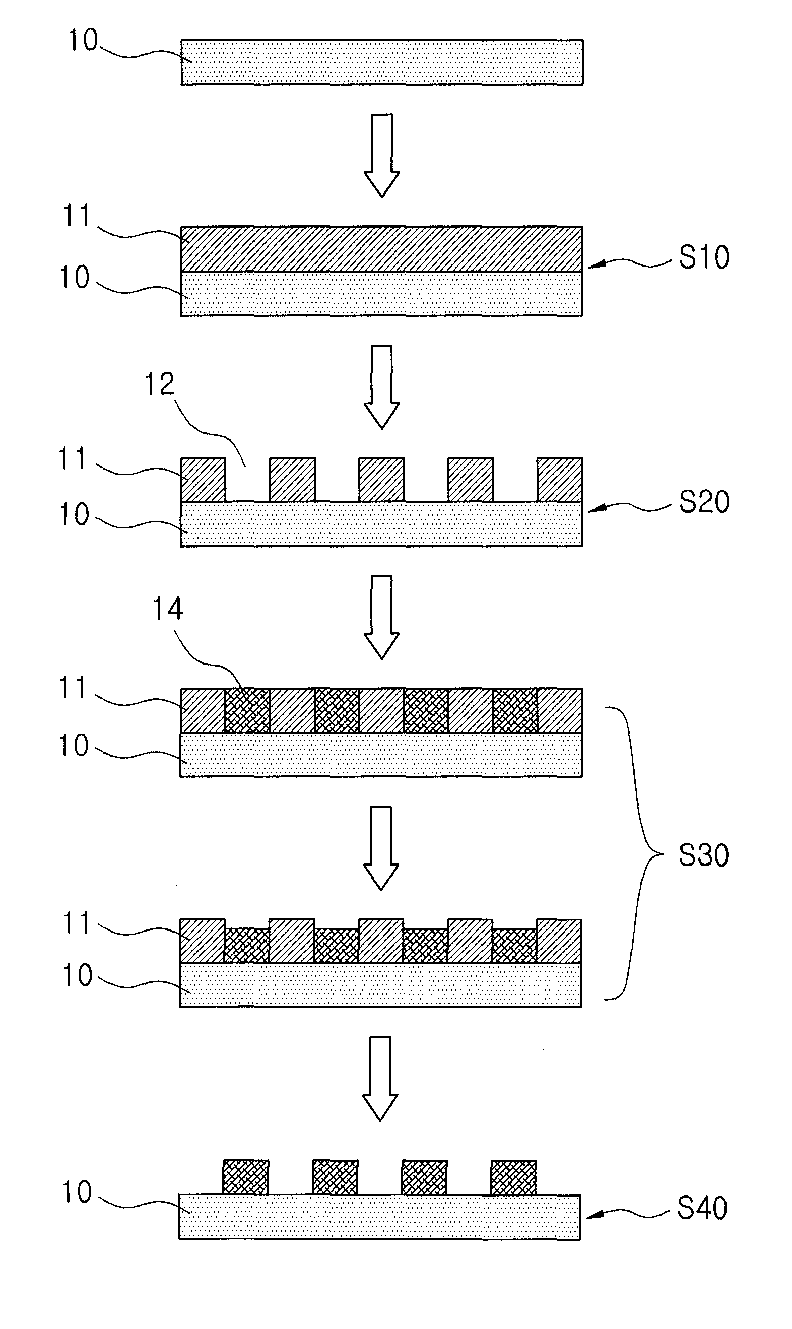
Examples
preparation example 1
Preparation of Silver Complex
[0080]Into a 250 ml Schlenk flask equipped with a stirrer, 34.89 g (129.8 mmol) of viscous liquid in which 2-ethylhexylammonium 2-ethylhexylcarbamate and butylammonium butylcarbamate are mixed at a molar ratio of 7:3 was put and 12.03 g (51.92 mmol) of silver oxide (made by Aldrich Chemical Co.) was added, followed by the reaction at room temperature for two hours with stirring. The reaction solution was initially a black slurry, but it turned transparent as complex was produced. Finally, 46.92 g of yellow, transparent aqueous silver complex was obtained and the silver complex had a viscosity of 7.8 pa·s and a silver content of 23.65 wt % (TGA analysis)
preparation example 2
Preparation of Silver Nanoparticles
[0081]Into a 100 ml beaker, 40.0 g of the silver complex prepared in Preparation Example 1 and 23.1 g of isopropyl alcohol were added and stirred at room temperature for ten minutes to prepare a first solution. Into another 100 ml beaker, 1.2 g of hydrazine monohydrate (made by Daejung Chemicals and Metals Co. Ltd.) and 50 g of isopropyl alcohol were added to prepare a second solution. The first solution and the second solution were injected into their inlets with a flow rate of 20 g / min, respectively. The solutions injected through the inlets were reacted at 5,000 rpm using a stirrer (made by Silverthorne, product name: L4RT-A) to obtain dark green slurry. The prepared slurry was filtered with a 1.2 um filter (made by Wattman company, product name: GF / C) by natural precipitation, followed by washing three times with isopropyl alcohol to obtain green nonopowder.
preparation example 3
Preparation of Conductive Ink
[0082]To 1.2 g of terpineol (made by TCI) as a solvent having a high boiling point, 40.0 g of the silver complex prepared by the same manner as described in Preparation Example 1 and 40 g of the green nanopowder prepared by the same manner as described in Preparation Example 2 were added and stirred for ten minutes, followed by adding 1.2 g of 1-amino-2-propanol (made by Aldrich Chemical Co.) and stirring again for tem minutes. After that, the resultant was passed through a three roll mill (made by Drais Manheim) three times to prepare a conductive ink composition having a silver content of 59.93 wt %.
PUM
| Property | Measurement | Unit |
|---|---|---|
| thickness | aaaaa | aaaaa |
| thickness | aaaaa | aaaaa |
| temperature | aaaaa | aaaaa |
Abstract
Description
Claims
Application Information