Nonvolatile storage element and manufacturing method thereof

a manufacturing method and storage element technology, applied in the direction of basic electric elements, bulk negative resistance effect devices, electric devices, etc., can solve the problems of difficult etching in the electrode processing process, difficult reduction of material cost, and degraded element characteristics by oxidation

Active Publication Date: 2012-10-04
CANON ANELVA CORP
View PDF4 Cites 16 Cited by
  • Summary
  • Abstract
  • Description
  • Claims
  • Application Information

AI Technical Summary

Benefits of technology

[0021]According to the present invention, it is possible to realize an electrode suitable for a variable resistance no...

Problems solved by technology

However, the following problems are present on the technologies described above.
Firstly, the technology that uses the Pt electrode as the electrode of the variable resistance element as disclosed in non-patent document 1, is effective in reducing the instability of the operation in the characteristic of the element resulting from the oxidation of the electrode, but has problems that etching is difficult in an electrode processing process and reducing the material cost is difficult.
Secondly, in the method disclosed in non-patent document 4, the technology using the TiN electrode as the electrode material is eff...

Method used


Image

  • Nonvolatile storage element and manufacturing method thereof
  • Nonvolatile storage element and manufacturing method thereof
  • Nonvolatile storage element and manufacturing method thereof

Examples


first embodiment

[0062]A first embodiment of the present invention will be described in detail with reference to accompanying drawings.

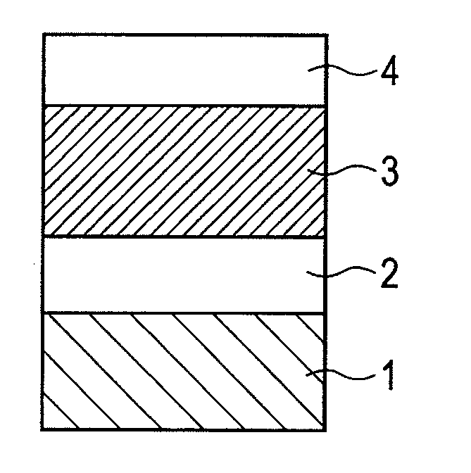
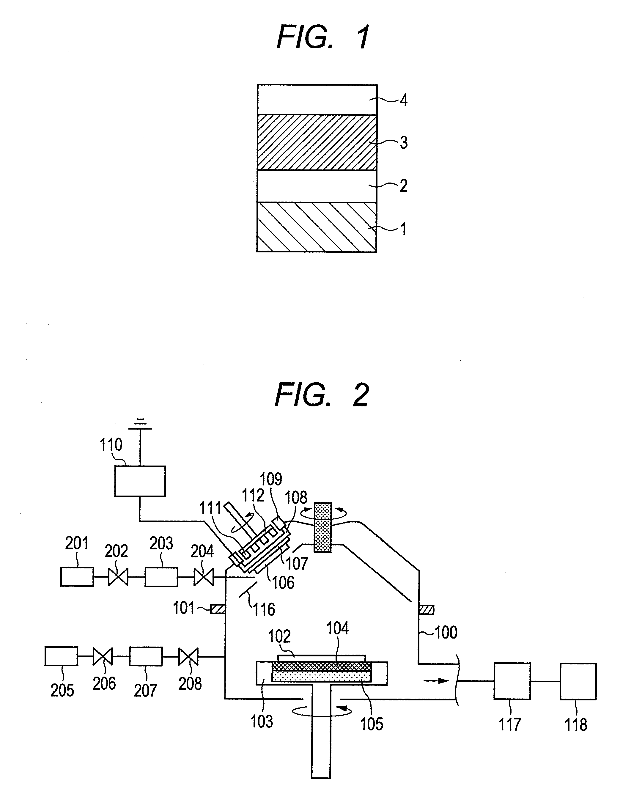
[0063]FIG. 7 is a schematic cross-sectional view of the structure of an element according to the first embodiment. On a silicon substrate 11 having a silicon oxide layer of 100 nm thick on its surface, with the processing device shown in FIG. 2, at an argon gas flow rate of 10 sccm and at a nitrogen gas flow rate of 10 sccm, an titanium nitride film 12 of 20 nm in which the mole ratio (N / Ti ratio) between Ti and N is 1.15 or more and the crystalline orientation X satisfies 1.213 formed of a metallic oxide containing Hf and Al is formed.

[0064]Then, by the same method as the titanium nitride film 12, a titanium nitride film 14 is deposited on the variable resistance layer 13. Then, lithography technology and RIE (reactive ion etching) technology were used to process the TiN film into a desired size.

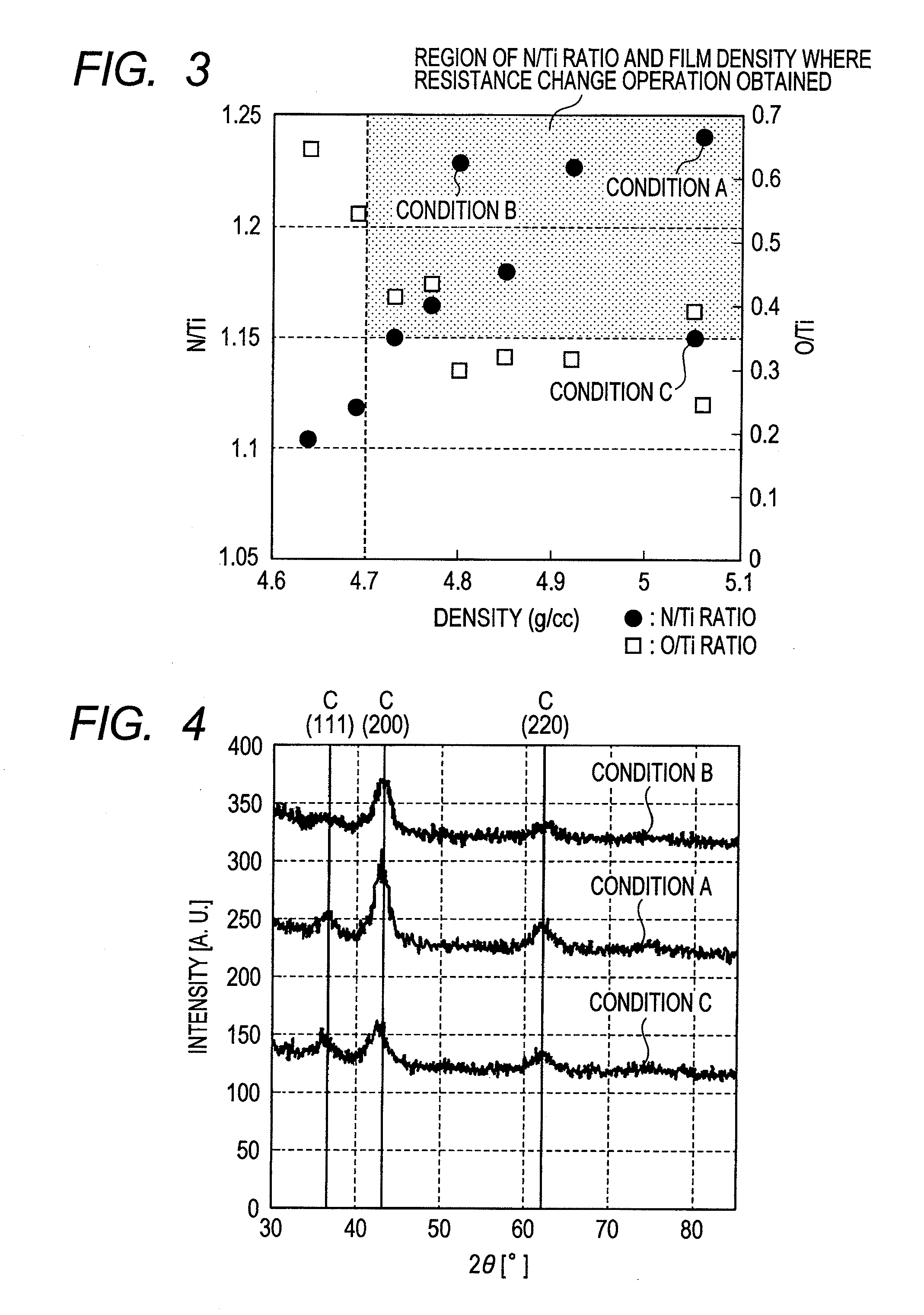
[0065]The composition of the deposited titanium nitride film was analyz...


PUM


Abstract

In a variable resistance nonvolatile storage element, an electrode suitable for a variable resistance operation and formed of a metallic nitride layer containing Ti and N is provided. In a nonvolatile storage device including: a first electrode; a second electrode; and a variable resistance layer which is sandwiched between the first electrode and the second electrode and in which a resistance value changes to two different resistance states, at least one of the first electrode and the second electrode is an electrode including a metallic nitride layer containing at least Ti and N, and a mole ratio (N/Ti ratio) between Ti and N in at least a part of the metallic nitride layer, the part being in contact with the variable resistance layer is 1.15 or more and a film density is 4.7 g/cc or more.

Description

CROSS-REFERENCES TO RELATED APPLICATIONS[0001]This application is a continuation application of International Application No. PCT / JP2010 / 067561, filed Oct. 6, 2010, which claims the benefit of Japanese Patent Application No. 2009-246134, filed Oct. 27, 2009. The contents of the aforementioned applications are incorporated herein by reference in their entities.TECHNICAL FIELD[0002]The present invention relates to a nonvolatile storage element and a manufacturing method thereof, and more particularly relates to a variable resistance nonvolatile storage element and a technology on a manufacturing method thereof.BACKGROUND ART[0003]A flash memory that is mainstream at present and that uses a floating gate, has a problem that as the size of a memory cell is reduced, variations in threshold voltage (Vth) occur due to interference by capacitive coupling between the floating gates of adjacent cells. Hence, as a memory suitable for the reduction in size, a variable resistance nonvolatile sto...

Claims


Application Information

Patent Timeline
IPC IPC(8): H01L47/00
CPCH01L45/08H01L45/1233H01L45/1641H01L45/146H01L45/1625H01L45/1253H10N70/24H10N70/841H10N70/041H10N70/026H10N70/8833H10N70/826H10N70/20
Inventor NAKAGAWA, TAKASHIKIM, EUN-MIOTANI, YUICHIKITANO, NAOMU
Owner CANON ANELVA CORP
Why Eureka
Try Eureka