Method for fabricating single-crystal GaN based substrate

a technology gan based substrate, which is applied in the direction of single crystal growth, polycrystalline material growth, chemistry apparatus and processes, etc., can solve the problems of high cost of fabricating a large size gan based substrate, long process time, and high cost of large-scale gan based substrate, etc., to achieve simple etching, easy separation of gan based substrate, and simple fabrication process

Inactive Publication Date: 2008-01-24
NAT CENT UNIV
View PDF37 Cites 17 Cited by
  • Summary
  • Abstract
  • Description
  • Claims
  • Application Information

AI Technical Summary

Benefits of technology

[0005]The main purpose of the present invention is to easily separate a GaN based substrate from a base substrate by a simple etching with a simple fabrication process and a low cost.

Problems solved by technology

Yet a disadvantage of this method is about applying the laser to heat the interface for the separation, which results in a long time of process and a high cost when fabricating a large size GaN based substrate.
All these steps take time and cost much.
The above prior arts both fabricate a GaN based substrate accompanying a longtime of processing and a high cost.
Hence, the prior arts do not fulfill users' requests on actual use.

Method used


Image

  • Method for fabricating single-crystal GaN based substrate
  • Method for fabricating single-crystal GaN based substrate
  • Method for fabricating single-crystal GaN based substrate

Examples


Embodiment Construction

[0020]The following description of the preferred embodiment is provided to understand the features and the structures of the present invention.

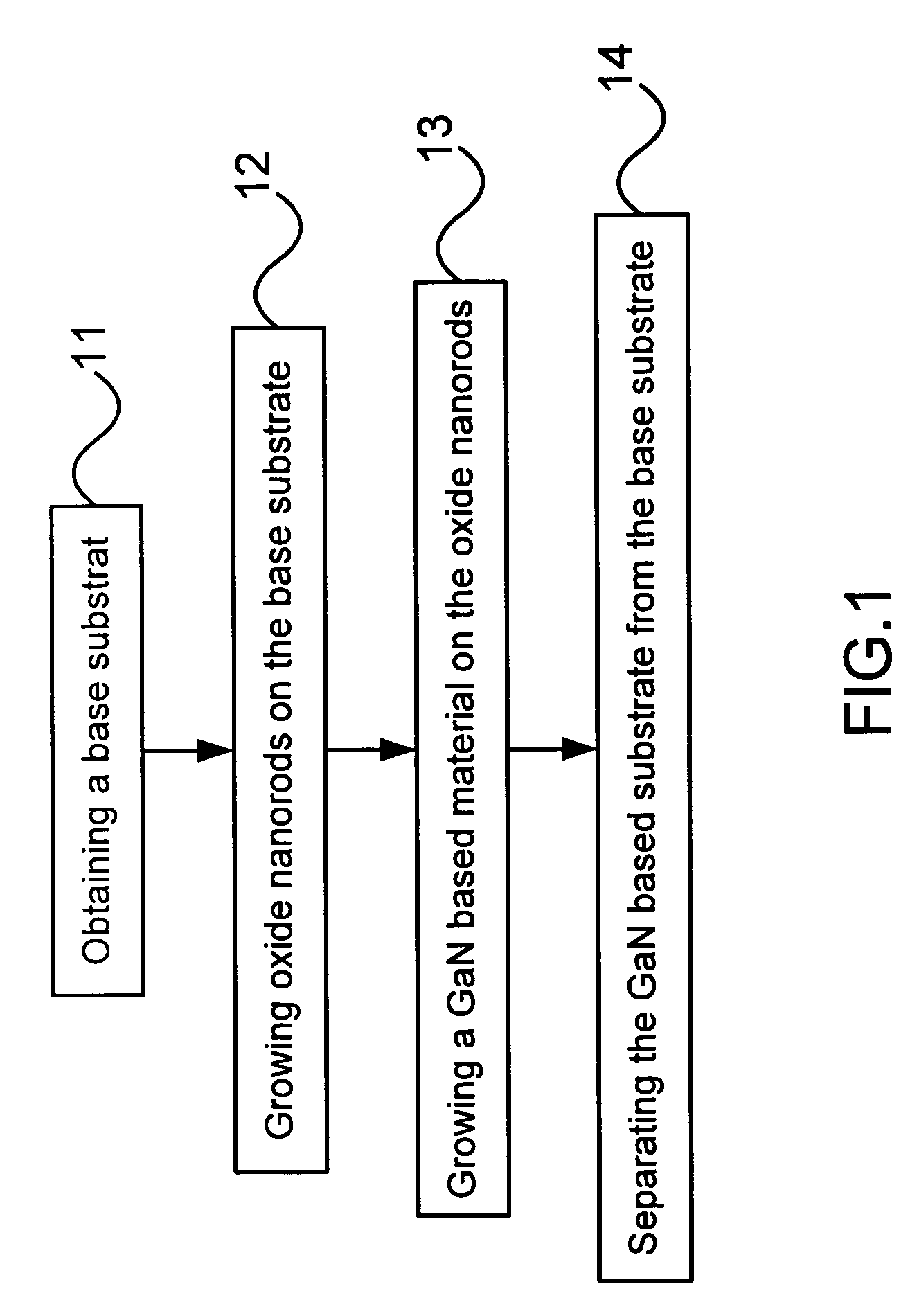
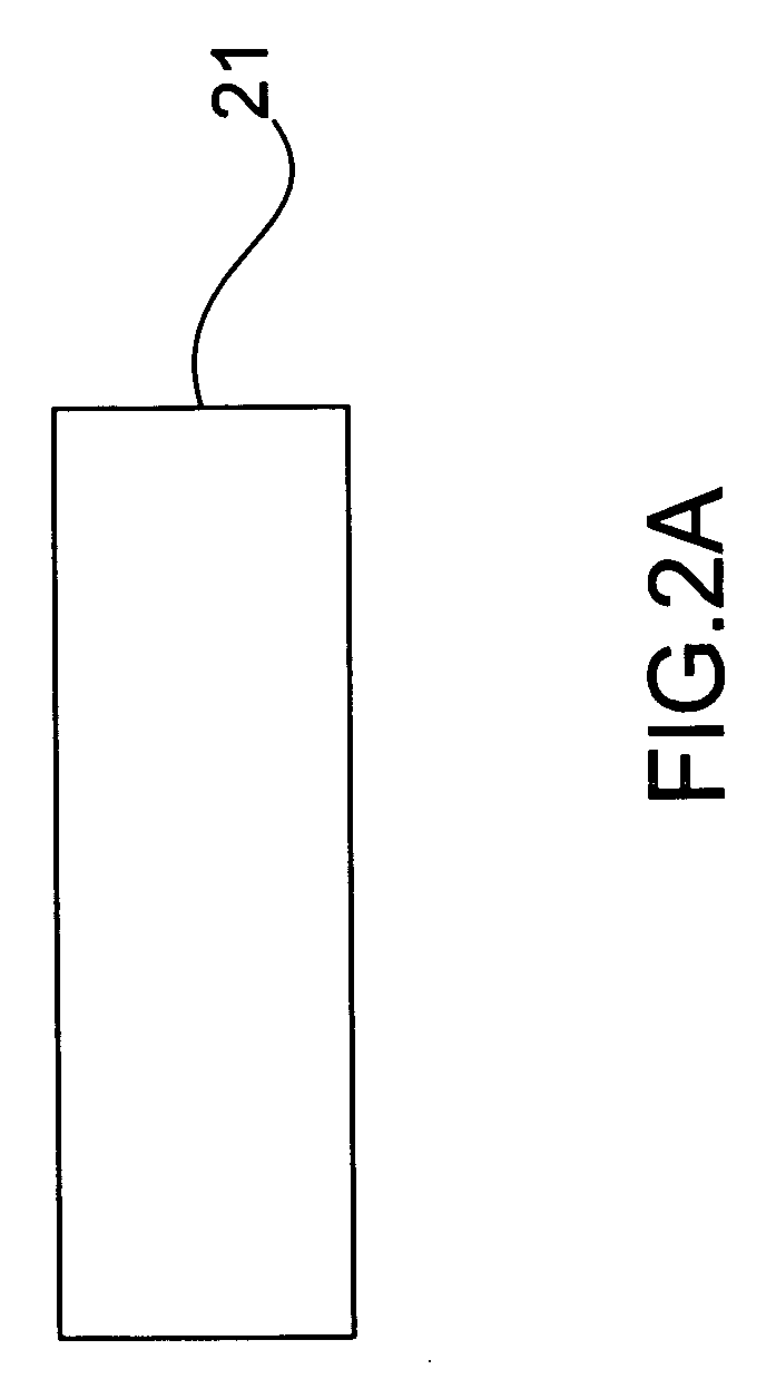
[0021]Please refer to FIG. 1 and FIG. 2A to FIG. 2D, which are views showing a flow chart of the preferred embodiment and structures in step (a), step (b), step (c) and step (d) separately according to the present invention. As shown in the figures, the present invention is a method for fabricating single-crystal GaN based substrate, comprising the following steps:

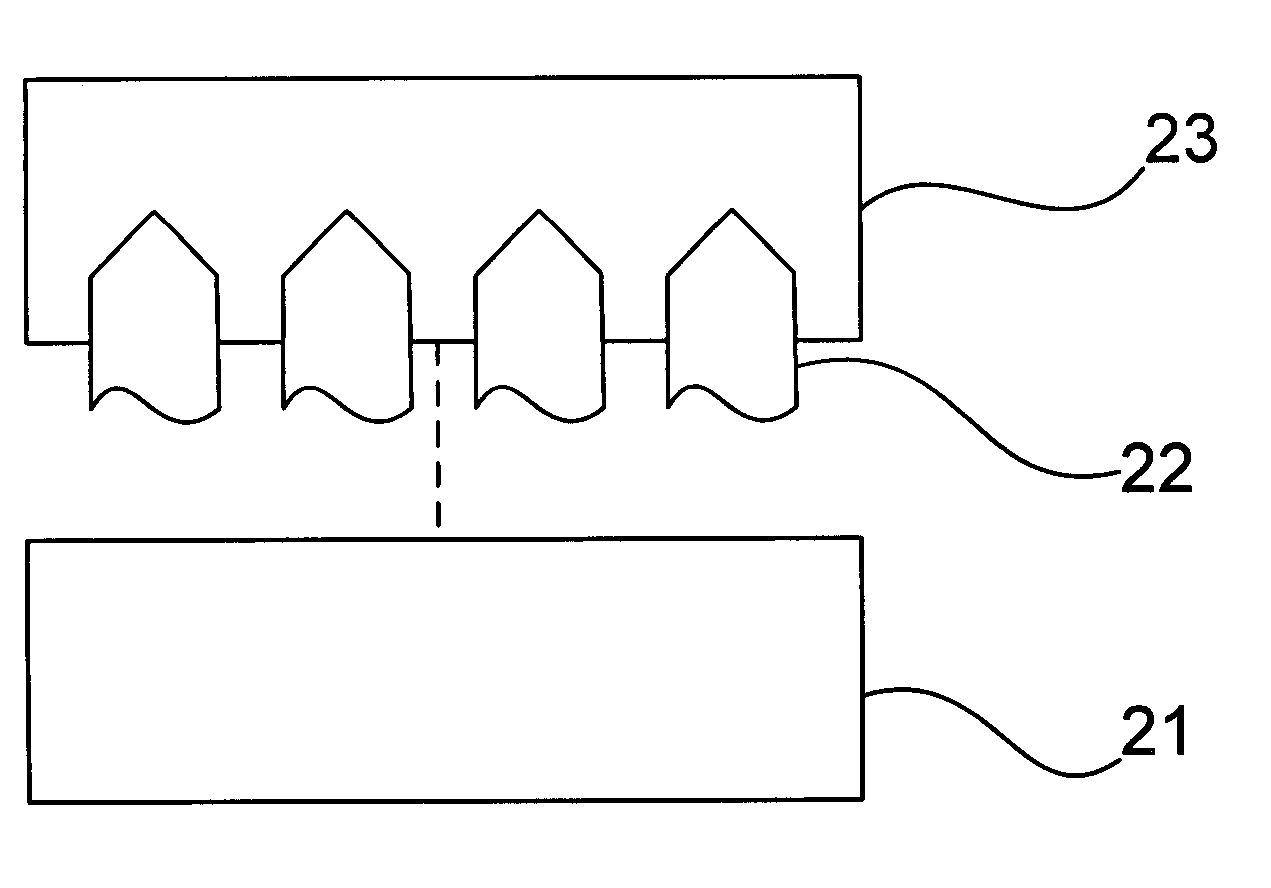
[0022](a) Obtaining a base substrate 11: A base substrate 21 is obtained from a material of sapphire, MgO, ZnO, Si, quartz, SiC or GaAs.

[0023](b) Growing oxide nanorods on the base substrate 12: Oxide nanorods 22 are grown on the base substrate 21, where the growth of the oxide nanorods is obtained by a molecular beam epitaxy, a metal-organic chemical vapor deposition or a hydride vapor phase epitaxy; the oxide nanorods 22 is made of ZnO, MgO, MgZnO, LiAlO2, LiGaO2, Li2SiO3, Li2GeO3...


PUM

PropertyMeasurementUnit
lengthaaaaaaaaaa
structureaaaaaaaaaa
stressaaaaaaaaaa

Abstract

A GaN based substrate is obtained with a simple etching. The GaN based substrate is separate from another base substrate with the etching. The whole process is easy and costs low. The substrate is made of a material having a matching lattice length for a lattice structure so that the substrate has good characteristics. And the GaN based substrate has good heat dissipation so that the stability and life-time of GaN based devices on the GaN based substrate are enhanced even when they are constantly operated under a high power.

Description

FIELD OF THE INVENTION[0001]The presented invention relates to fabricating a substrate; more particularly, relates to easily separating a GaN based substrate from a base substrate.DESCRIPTION OF THE RELATED ARTS[0002]A prior art of a substrate of single crystal GaN is obtained through a metal-organic chemical vapor deposition or a hydride vapor phase epitaxy, where a GaN based material is deposited on a base substrate and then the GaN based material is separated from the base substrate by illuminating the interface with a laser to obtain a single crystal GaN substrate, as shown in FIG. 3A and FIG. 3B. In another word, a general single crystal GaN substrate is obtained by firstly growing a GaN based material 32 on a base substrate 31. Then a laser 33 is applied to heat up an interface between the base substrate 31 and the GaN based material 32 to decompose the GaN into gallium and nitrogen. Then the base substrate 31 is heated to the melting point of gallium so that the GaN based mat...

Claims


Application Information

Patent Timeline
Patent Type & Authority Applications(United States)
IPC IPC(8): C30B23/00
CPCC30B23/02C30B25/02C30B29/605C30B29/403C30B29/406C30B29/16
Inventor CHYI, JEN-INNCHEN, GUAN-TING
Owner NAT CENT UNIV
Why Eureka
Try Eureka