Liquid crystal display device and method for fabricating the same

a technology of liquid crystal display and liquid crystal panel, which is applied in the direction of non-linear optics, instruments, optics, etc., can solve the problems of difficult bonding of sealing materials, difficult bonding of liquid crystal panels, and difficult bonding of organic substances, so as to improve the adhesion force of panels, minimize contact area, and maximize contact area

Inactive Publication Date: 2005-02-22
LG DISPLAY CO LTD
View PDF2 Cites 19 Cited by
  • Summary
  • Abstract
  • Description
  • Claims
  • Application Information

AI Technical Summary

Benefits of technology

An object of the present invention is to provide a liquid crystal display device with an improved adhesion force of a panel by minimizing a contact area between a sealing material and an organic passivation layer, and maximizing a contact area between the sealing material and an inorganic insulation layer by removing the organic passivation layer formed at a sealing region of a liquid crystal display device.
Another object of the present invention is to provide a method for fabricating a liquid crystal display device in which a patterning process of an insulation is performed through two steps such that a portion of an organic insulation layer of a sealing region is first removed in patterning an inorganic insulation layer of a pixel region and then the remaining organic insulation layer at the sealing region is removed in patterning the organic insulation layer of the pixel region, thereby forming an opening for filling a sealing material and improving an adhesion force of a panel.

Problems solved by technology

However, organic substances, such as photo acryl or BCB, and the sealing material do not easily bond together.
However, although the adhesion force of the liquid crystal panel is improved by forming the openings 62 at the inorganic passivation layer 39 and the organic passivation layer 37 between the metal layers 24, bonding of the liquid crystal panel is problematic.

Method used


Image

  • Liquid crystal display device and method for fabricating the same
  • Liquid crystal display device and method for fabricating the same
  • Liquid crystal display device and method for fabricating the same

Examples


Embodiment Construction

Reference will now be made in detail to the preferred embodiments of the present invention, examples of which are illustrated in the accompanying drawings.

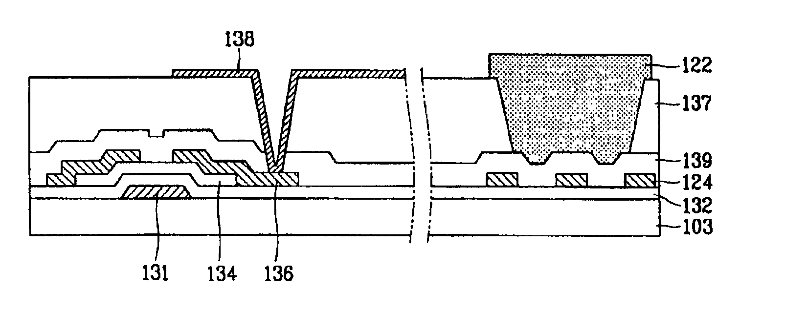
FIG. 4 is a cross sectional view of an exemplary sealing region of a liquid crystal display device in accordance with the present invention. In FIG. 4, an insulation layer 132 may be stacked upon a transparent substrate 103, and a plurality of metal layers 124 may be formed on the insulation layer 132. The metal layers 124 may be electrically connected to an external connecting pad (not shown). Alternatively, the metal layers 124 may be formed directly on the transparent substrate 103. An inorganic passivation layer 139 including inorganic substances may be formed on the metal layers 124, and an organic passivation layer 137 including organic substances may formed with an opening 162. The opening 162 may be formed to extend over at least two of the metal layers 124, and may extend over an entire sealing region of the transparent s...


PUM

PropertyMeasurementUnit
thicknessaaaaaaaaaa
sealing forceaaaaaaaaaa
weightaaaaaaaaaa

Abstract

A liquid crystal display device includes a first substrate having a plurality of thin film transistors and a plurality of metal lines, a first insulation material layer formed on the metal lines, a second insulation material layer formed on the first insulation material layer on the metal lines, a first hole formed in the second insulation material layer over at least two of the metal lines, a second contact hole formed in the first and second insulation layers exposing a drain electrode of the thin film transistors, a pixel electrode connected to the drain electrode through the second contact hole, a sealing material formed within the first hole, a second substrate bonded to the first substrate via the sealing material, and a liquid crystal material disposed between the first and second substrates.

Description

The present invention claims benefit of Korean Patent Application No. 89306 / 2001 filed in Korea on Dec. 31, 2001, which is hereby incorporated by reference.BACKGROUND OF THE INVENTION1. Field of the InventionThe present invention relates to a liquid crystal display device and, more particularly, to a liquid crystal display device having an improved attachment of a liquid crystal panel for improving a sealing force of a sealing material.2. Description of the Related ArtIn general, a liquid crystal display (LCD) device is a transmission-type flat panel display device adaptable to various electronic instruments, such as mobile phones, personal digital assistants (PDAs), notebook computers, and lap-top computers. Because of their light weight, thin profile, compact size, and high picture quality, the LCD device is advantageous as compared to other flat panel display devices. Generally, the LCD device can be categorized based upon its method for manipulating liquid crystal molecules. Pre...

Claims


Application Information

Patent Timeline
Patent Type & Authority Patents(United States)
IPC IPC(8): G02F1/13G02F1/1339G02F1/1362
CPCG02F1/1339G02F1/136227
Inventor KIM, WOO-HYUNHWANG, YONG-SUP
Owner LG DISPLAY CO LTD
Why Eureka
Try Eureka