Micromechanical optical switch

a micromechanical and optical switch technology, applied in optics, instruments, electrical apparatus, etc., can solve the problems of increasing the required drive voltage, limiting the ability of network designers to accomplish data communications in the optical domain, and micromechanical structures typically do not provide suitable speed or reliability for cost-effective commercial applications, etc., to achieve the effect of reducing problems or reducing problems

Inactive Publication Date: 2005-02-22
CHEETAH OMNI
View PDF78 Cites 87 Cited by
  • Summary
  • Abstract
  • Description
  • Claims
  • Application Information

AI Technical Summary

Benefits of technology

According to the teachings of the present invention, a micromechanical optical switch element is provided that substantially eliminates or reduces problems associated with prior systems.

Problems solved by technology

In comparison, the inability to selectively route logical signals that are transmitted in the optical domain has restricted the ability of network designers to accomplish data communications solely in the optical domain.
These micromechanical structures typically do not provide suitable speed or reliability for cost-effective commercial applications.
For example, many micromechanical structures suffer from air damping effects, which increase the required drive voltage and slow the operation of the device.
In addition, these devices have not been tunable to optimize switching speeds according to common packet sizes encountered by the switch.

Method used


Image

  • Micromechanical optical switch
  • Micromechanical optical switch
  • Micromechanical optical switch

Examples


Embodiment Construction

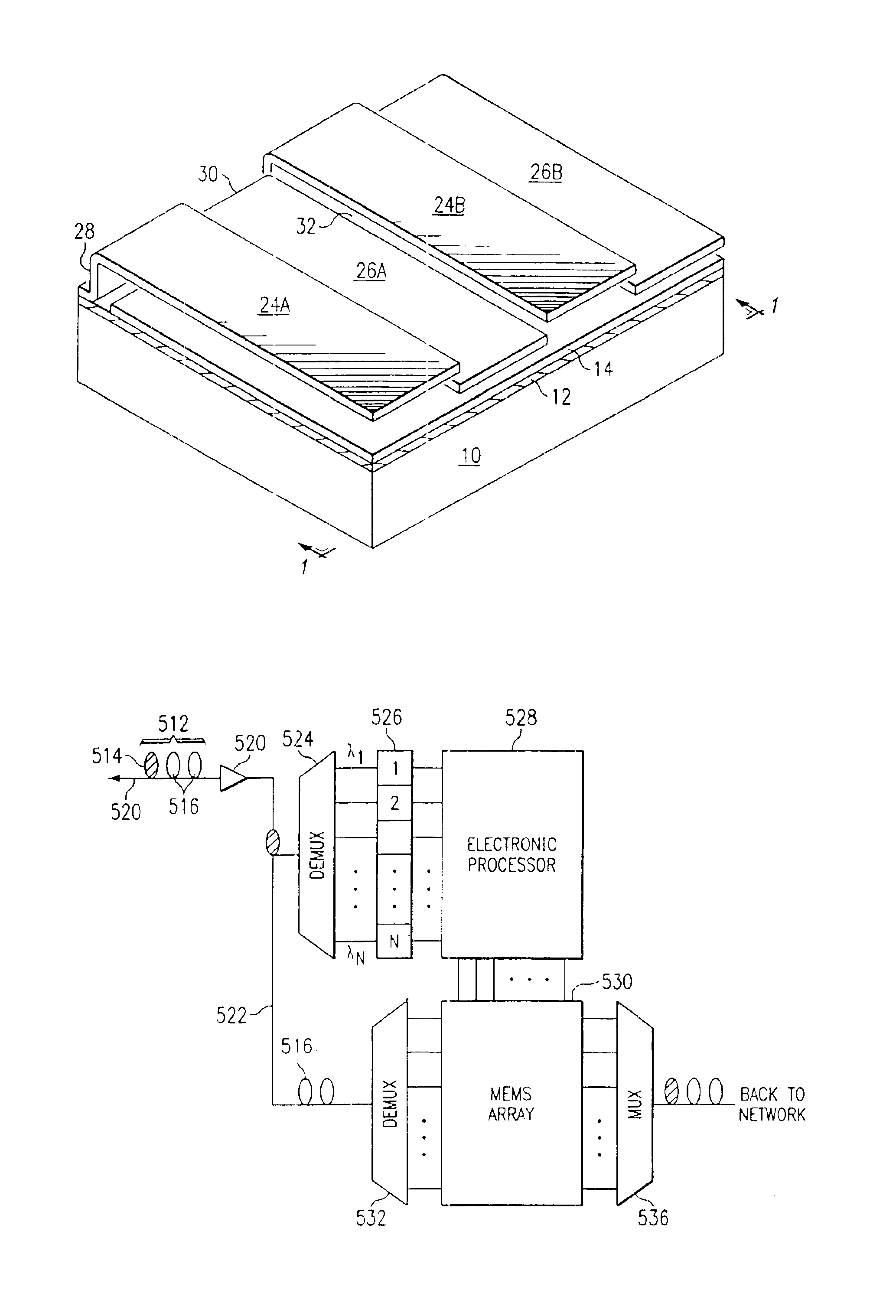
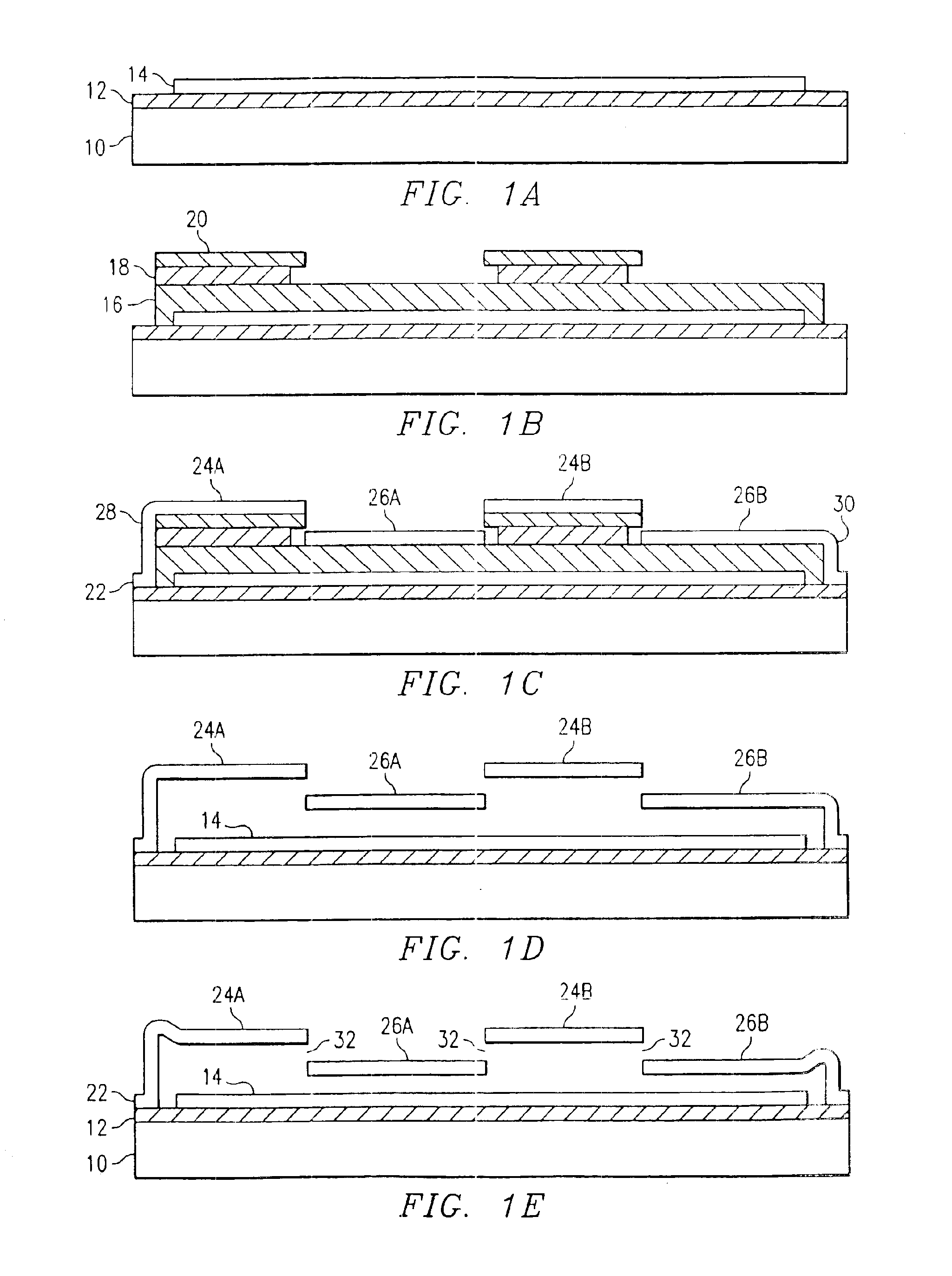
The optical switching element of the present invention is formed on an outer surface of a substrate 10 shown in FIG. 1A. Substrate 10 may comprise, for example, n-type silicon or indium phosphide. As will be described herein, in one mode of operation, it is advantageous if the substrate is optically transmissive in the wavelength range of the optical signal to be switched by the element. To facilitate that mode of operation, in a particular embodiment, a single crystalline silicon substrate can be manufactured so that it is optically transmissive in the range of wavelengths between approximately 1,300 to approximately 1,700 nanometers with an optimal transmissive wavelength of approximately 1,500 nanometers.

Referring again to FIG. 1A, an antireflective layer 12 is deposited or grown on an outer surface of the substrate 10. Antireflective layer 12 may comprise, for example, a layer of silicon nitride. In the illustrated embodiment, layer 14 is formed to be one-quarter wavelength in o...


PUM


Abstract

An optical switch element is described, which includes a fixed layer disposed outwardly from a substrate and a movable mirror assembly disposed outwardly from the fixed layer. The moveable mirror assembly is operable to move relative to the fixed layer responsive to a voltage applied to the movable mirror assembly. In a particular embodiment, the movable mirror assembly includes an inner strip spaced apart from the fixed layer by a first distance and an outer strip disposed approximately adjacent to the inner strip and spaced apart from the fixed layer by a second distance which is greater than the first distance. The optical transmission of the optical switch element changes depending on the position of the movable mirror assembly.

Description

TECHNICAL FIELD OF THE INVENTIONThis invention relates in general to the field of electro-optical systems and more particularly to an improved optical switch element and methods of forming and using the element.BACKGROUND OF THE INVENTIONThe ability to transmit information in the optical domain has greatly enhanced the speed and bandwidth of data communications. In comparison, the inability to selectively route logical signals that are transmitted in the optical domain has restricted the ability of network designers to accomplish data communications solely in the optical domain. Accordingly, before a signal can be routed or switched it must first be converted into electrical signals which can be logically processed using conventional electrical digital computing systems.There have been a number of attempts to create a workable optical switch architecture which allows for the selective routing of light beams carrying data communications. Some of these solutions have involved the form...

Claims


Application Information

Patent Timeline
Patent Type & Authority Patents(United States)
IPC IPC(8): G02B26/08G02B6/35G02B6/34G02B26/00G03H1/00H04Q11/00
CPCG02B6/352G02B26/001G02B26/0833G02B26/0841H04Q11/0005G02B6/3516G02B6/3512H04Q2011/0077G02B6/3518G02B6/3546G02B6/3548G02B6/3552G02B6/356G02B6/357G02B6/3584H04Q11/0066H04Q2011/0015H04Q2011/0016H04Q2011/002H04Q2011/0039
Inventor ISLAM, MOHAMMED N.KUDITCHER, AMOS
Owner CHEETAH OMNI
Why Eureka
Try Eureka