Method of reducing trench aspect ratio

Active Publication Date: 2005-03-01
NAN YA TECH
View PDF11 Cites 4 Cited by
  • Summary
  • Abstract
  • Description
  • Claims
  • Application Information

AI Technical Summary

Benefits of technology

Another object of the present invention is to provide a method for lowering the aspect ratio of a trench during a deposition process to fill the trench without creating voids.
In order to achieve these objects, the present invention provides a method of reducing the aspect ratio of a trench. A trench is formed in a substrate. Using HDP-CVD, a conformal first oxide layer is formed on a surface of the trench. A conformal first nitride layer is formed on the first oxide layer. A portion of the first nitride layer is removed to cause the first nitride layer to be lower than a top surface of the substrate. Using a BOE solution, the first nitride layer and a portion of the first oxide layer are removed and thus leave a remaining first oxide layer on a lower portion of the surface of the trench.
Moreover, when the aspect ratio of the trench is high, subsequent to the above steps, at least one cycle of the following steps can be performed. Using HDP-C

Problems solved by technology

Such a void 20 seriously affects device reliability and yie

Method used


Image

  • Method of reducing trench aspect ratio
  • Method of reducing trench aspect ratio
  • Method of reducing trench aspect ratio

Examples


Example

A preferred embodiment of the invention will now be described in detail with reference to the accompanying drawings.

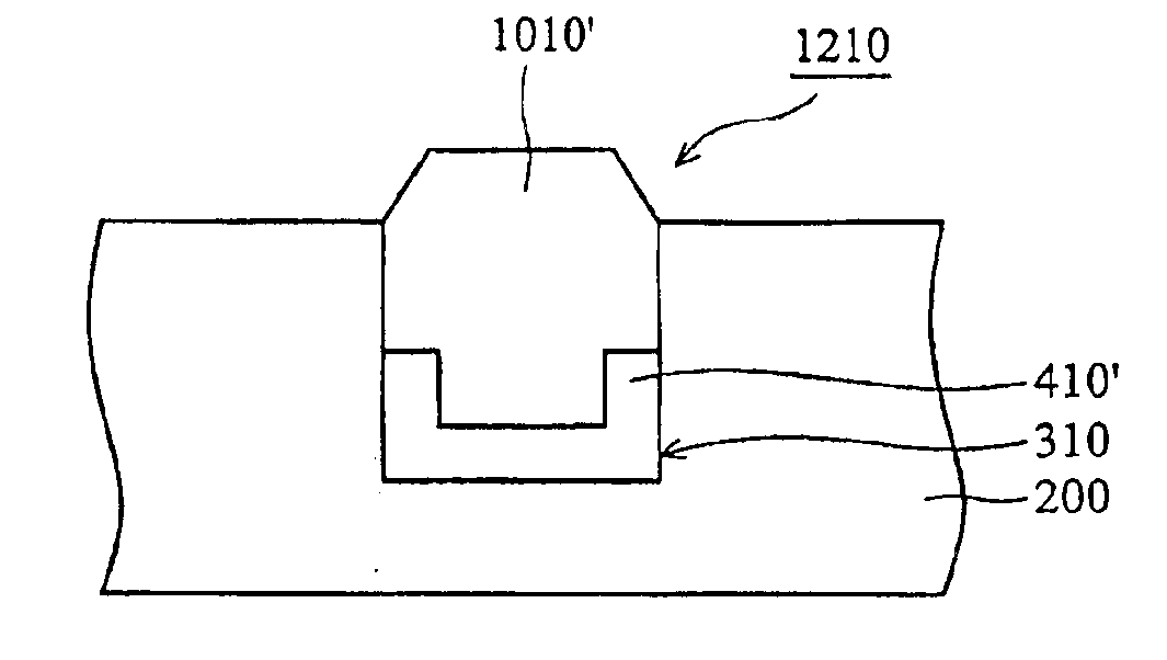
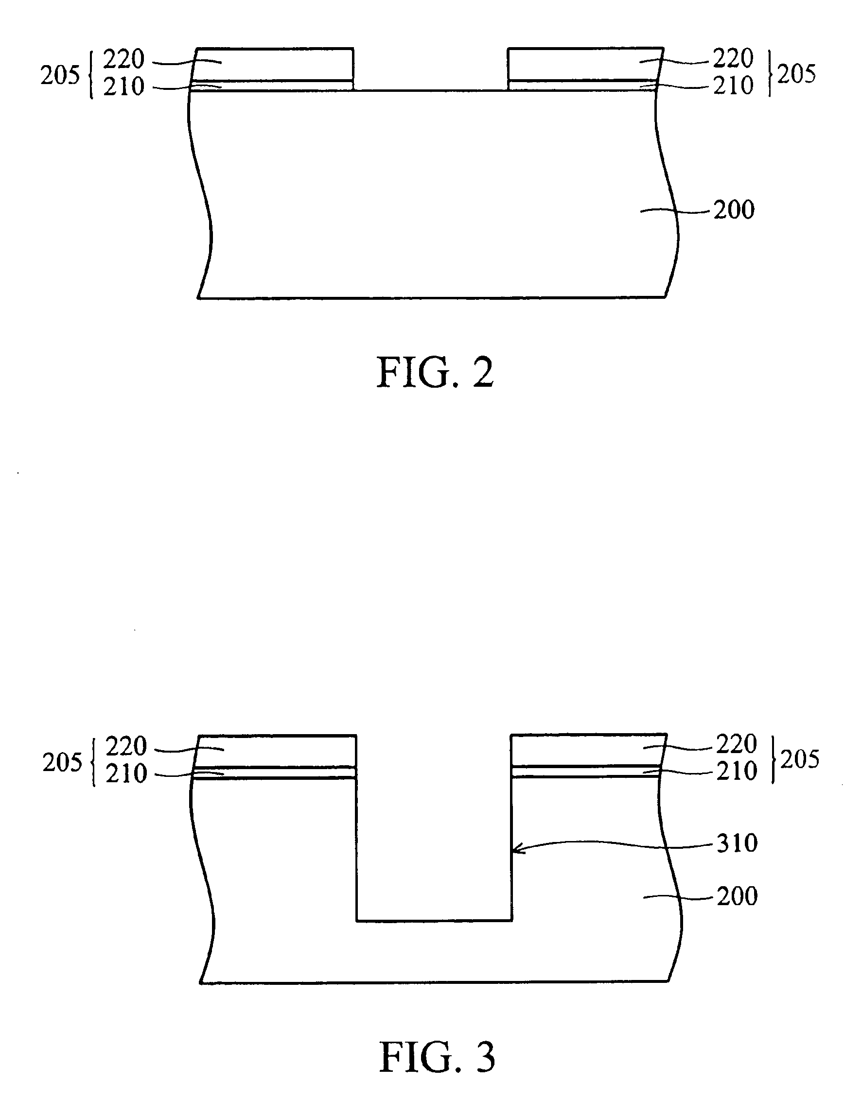
FIGS. 2˜12 are sectional views showing the trench isolation process of the present invention.

In FIG. 2, a semiconductor substrate 200, such as a silicon wafer, is provided. A shield layer 205 preferably comprising a pad oxide layer 210 and a silicon nitride layer 220 is formed on part of the substrate 200. The pad oxide layer 210 can be a SiO2 layer formed by thermal oxidation or CVD (chemical vapor deposition). The silicon nitride layer 220 can be a Si3N4 layer formed by CVD. For example, the thickness of the pad oxide layer 210 is about 100 Å and the thickness of the silicon nitride layer 220 is about 900 Å. The shield layer 205 serves as a stacked mask for defining an isolation area in the substrate 200.

In FIG. 3, using the shield layer 205 as a mask, part of the substrate 200 is etched to form a trench 310. The depth of the trench 310 is, for example, 2600˜5000 Å. ...


PUM


Abstract

A method of reducing trench aspect ratio. A trench is formed in a substrate. Using HDP-CVD, a conformal first oxide layer is formed on a surface of the trench. A conformal first nitride layer is formed on the first oxide layer. Part of the first nitride layer is removed to cause the first nitride layer to be lower than a top surface of the substrate. Using a BOE solution, the first nitride layer and part of the first oxide layer are removed to leave a remaining first oxide layer on the lower portion of the surface of the trench. Thus, the trench aspect ratio is reduced.

Description

BACKGROUND OF THE INVENTION1. Field of the InventionThe present invention relates to a semiconductor manufacturing process, and more particularly, to a method of reducing the aspect ratio of a trench.2. Description of the Related ArtSemiconductor device geometry continues to decrease in size, providing more devices per fabricated wafer. Currently, some devices are fabricated with less than 0.25 μm spacing between features; in some cases there is as little as 0.18 μm spacing between features, which often takes the form of a trench.An isolation technique called shallow trench isolation (STI) has been introduced to the fabrication of devices to reduce size. Isolation trenches are formed in a substrate between features, such as transistors. FIGS. 1A˜1B are schematic views of a traditional STI process.In FIG. 1A, a substrate 10 such as a silicon wafer is provided. A shield layer 11 comprising a pad oxide layer 12 and a silicon nitride layer 14 is formed on part of the substrate 10. The s...

Claims


Application Information

Patent Timeline
IPC IPC(8): H01L21/762H01L21/70H01L21/02H01L21/316H01L21/318H01L21/314H01L21/311
CPCH01L21/02164H01L21/02274H01L21/02362H01L21/76224H01L21/31612H01L21/3144H01L21/3185H01L21/31116
Inventor WU, CHANG-RONGWU, SENG-HSIUNGCHEN, YI-NAN
Owner NAN YA TECH
Why Eureka
Try Eureka