
Semiconductor integrated circuit for phase management of clock domains including PLL circuit

Inactive Publication Date: 2005-03-01
RENESAS ELECTRONICS CORP
View PDF5 Cites 4 Cited by
  • Summary
  • Abstract
  • Description
  • Claims
  • Application Information

AI Technical Summary

Benefits of technology

[0013]An object of the present invention is to provide a semiconductor integrated circuit device capable of performing easy and highly accurate phase management between clock domains to which clocks having different frequencies from each other are inputted.
[0015]The phase comparator provided on the first and second phase comparison loops can compare the delay provided for the first variable delay circuit on the first and second phase comparison loops with the delay provided for the second variable delay circuit on the second phase comparator loop, thereby providing the comparison result for the second variable delay circuit. This allows easy and highly accurate phase management to be performed between the clock domains without estimating delay values at the respective clock domains by circuit simulations.

Problems solved by technology

Thus, a problem arises in that estimating delay values by circuit simulations is time-consuming, causing the design period to be prolonged.

Method used


Image

  • Semiconductor integrated circuit for phase management of clock domains including PLL circuit
  • Semiconductor integrated circuit for phase management of clock domains including PLL circuit
  • Semiconductor integrated circuit for phase management of clock domains including PLL circuit

Examples


Embodiment Construction

ferred embodiment of the present invention;

[0030]FIG. 14 is a circuit diagram showing phase management according to an eighth preferred embodiment of the present invention;

[0031]FIG. 15 is a circuit diagram showing a PLL circuit according to the eighth preferred embodiment;

[0032]FIG. 16 is a circuit diagram showing phase management according to a ninth preferred embodiment of the present invention;

[0033]FIG. 17 is a circuit diagram showing a phase comparator according to the ninth preferred embodiment;

[0034]FIG. 18 is a timing chart showing the phase management according to the ninth preferred embodiment; and

[0035]FIG. 19 is a circuit diagram showing conventional phase management.

DESCRIPTION OF THE PREFERRED EMBODIMENTS

[0036]First Preferred Embodiment

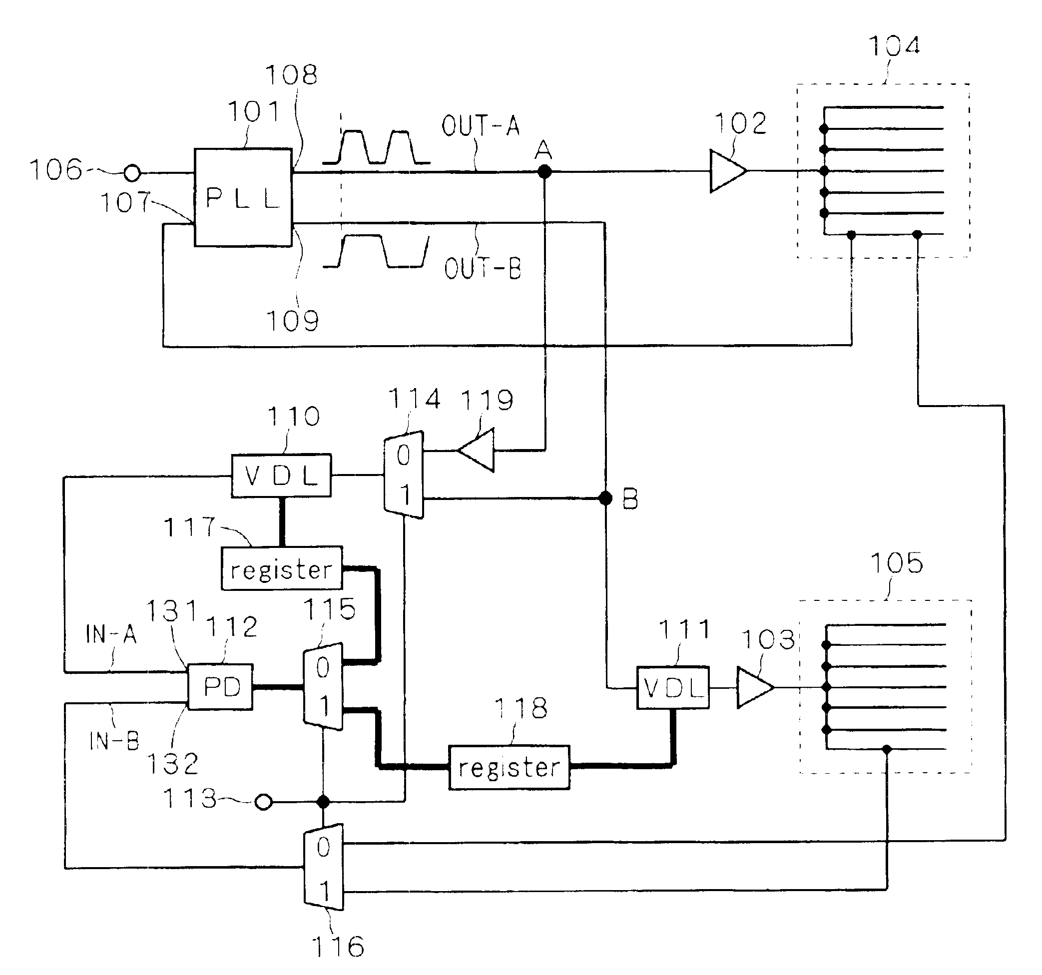
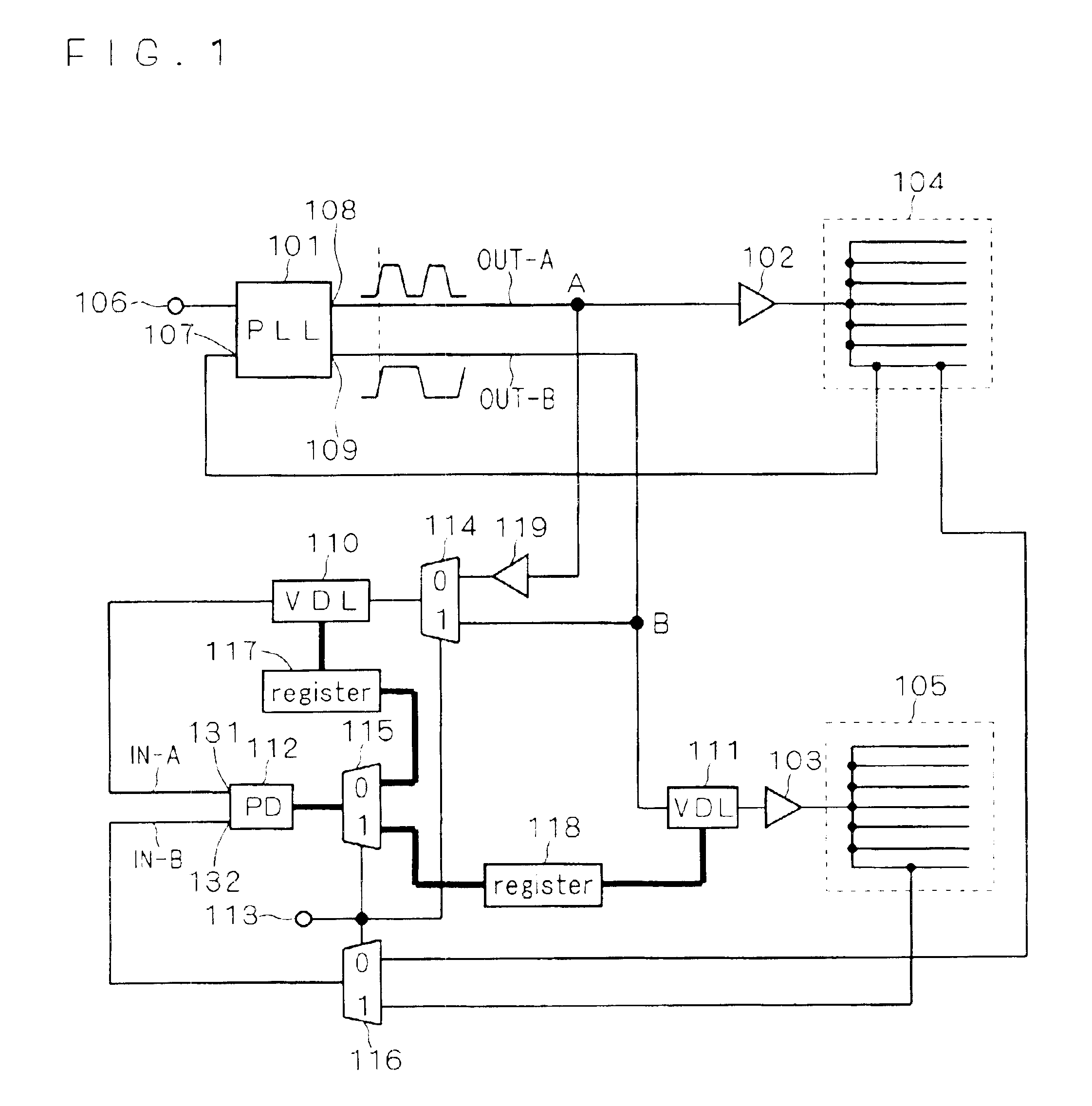
[0037]FIG. 1 is a circuit diagram showing phase management between a plurality of clock domains in a semiconductor integrated circuit according to a first preferred embodiment of the present invention.

[0038]A PLL circuit 101 includes a ...


PUM


Abstract

Assuming that clocks in an A clock driver (102), a B clock driver (103) and a CMOS buffer circuit (119) have delay values Ta, Tb and Td, respectively, a delay value Ta−Td is stored in a register circuit (117) when terminals “0” of selector circuits (114, 115, 116) are selected, and a delay value Ta−Td−Tb is stored in a register circuit (118) when the terminals “0” are switched to “1”. Thus, determining a delay value at the CMOS buffer circuit (119) allows a phase difference between the A clock driver (102) and B clock driver (103) to be determined.

Description

BACKGROUND OF THE INVENTION[0002]1. Field of the Invention[0003]The present invention relates to a semiconductor integrated circuit, and more particularly, to a technique of performing easy and highly accurate phase management between a plurality of clock domains in synchronization with each other by means of a PLL (phase locked loop) circuit.[0004]2. Description of the Background Art[0005]FIG. 19 is a circuit diagram showing phase management between a plurality of clock domains in a conventional semiconductor integrated circuit which operates in synchronization with clock signals.[0006]A PLL circuit 501 includes a reference clock input terminal 506 to which a reference clock is inputted and a feedback clock input terminal 507 to which a feedback clock is inputted. The PLL circuit 501 further includes an A clock output terminal 508 outputting an A clock, which is connected to an input terminal of a CMOS buffer circuit 510. An A clock from the A clock output terminal 508 will be refe...

Claims


Application Information

Patent Timeline
IPC IPC(8): H03K5/13H03K19/0175H03L7/087H03L7/06H03K5/00H03L7/08H03L7/16H03L7/22H03L7/00H03L7/07H03L7/081H03L7/099
CPCH03K5/133H03L7/0996H03L7/0814H03L7/07H03K2005/00071H03L7/08
Inventor HIROTA, TAKANORIISHIBASHI, ATSUHIKO
Owner RENESAS ELECTRONICS CORP
Learn More