Signal transmission circuit and electronic equipment

a transmission circuit and signal technology, applied in the direction of line-transmission details, cross-talk/noise/interference reduction, multiple-port network, etc., can solve the problem that the capacitor b>1/b> does not work effectively for eliminating noise components

Inactive Publication Date: 2005-03-01
FUJITSU GENERAL LTD
View PDF9 Cites 10 Cited by
  • Summary
  • Abstract
  • Description
  • Claims
  • Application Information

AI Technical Summary

Benefits of technology

An object of the invention is to provide a signal transmission circuit for eliminating noise components superposed on signals and electronic equipment that comprises the signal transmission circuit, without adding a part for eliminating noise components in signals, by using a constitution of a printed wiring board, and to provide an electronic equipment including the signal transmission circuit.
According to the invention, in the signal transmission circuit, a signal transmission path between the capacitor for eliminating noise components of signals and the input terminal section is constituted by only a conductive pattern. Consequently, the capacitor for eliminating noise components effectively functions, so that it is possible to sufficiently eliminate noise components from signals transmitted in the signal transmission circuit.
According to the invention, in the signal transmission circuit, in a signal transmission path between the capacitor for eliminating noise components of signals and the transistor for signal transmission, two or more via holes or through holes are included. Consequently, not only the capacitor but also the transmission path from the capacitor to the transistor serves for eliminating noise, so that it is possible to sufficiently eliminate noise components from signals transmitted in the signal transmission circuit.
According to the invention, in the signal transmission circuit, a signal transmission path between the capacitor for eliminating noise components of signals and the transistor for signal transmission is placed in the vicinity of the grounding wiring. Consequently, the transmission path between the capacitor and the transistor and the grounding wiring function as a capacitor for eliminating noise components, so that noise components are sufficiently eliminated from signals transmitted in the signal transmission circuit.
According to the invention, in the signal transmission circuit, in a signal transmission path between the two capacitors for eliminating noise components of signals, one or more via holes or through holes are included. Consequently, not only the two capacitors but also the transmission path between the capacitors serves for eliminating noise, so that it is possible to further sufficiently eliminate noise components from signals transmitted in the signal transmission circuit.
As described above, according to the invention, the signal transmission circuit is interposed between the input terminal section and the processing circuit section, and at least the first capacitor is connected to the input wiring from the input terminal section to the base terminal of the transistor. In the input wiring, a leading-side transmission path between the first capacitor and the input terminal section is constituted by only a conductive pattern. Moreover, according to the invention, the resistor is further connected to the input wiring. In an intermediate transmission path from the connection point with the first capacitor to the connection point with the resistor in the input wiring, two or more via holes or through holes are included. Further, according to the invention, the intermediate transmission path is placed in the vicinity of the grounding wiring. Furthermore, according to the invention, the second capacitor is further connected to the intermediate transmission path of the input wiring, and one or more via holes or through holes are included in a portion of the input wiring between the two capacitors. On the basis of the above reasons, it is possible to further sufficiently eliminate noise components from signals transmitted in the signal transmission circuit. Besides, according to the invention, the electronic equipment comprises the aforementioned signal transmission circuit. Consequently, an influence of noise components on signal processing in the signal processing section is sufficiently suppressed.

Problems solved by technology

Consequently, there is a possibility that the capacitor 1 does not function effectively for eliminating noise components.

Method used


Image

  • Signal transmission circuit and electronic equipment
  • Signal transmission circuit and electronic equipment
  • Signal transmission circuit and electronic equipment

Examples


first embodiment

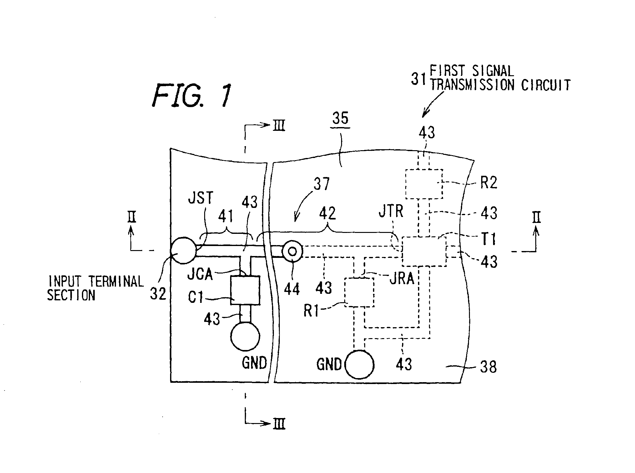
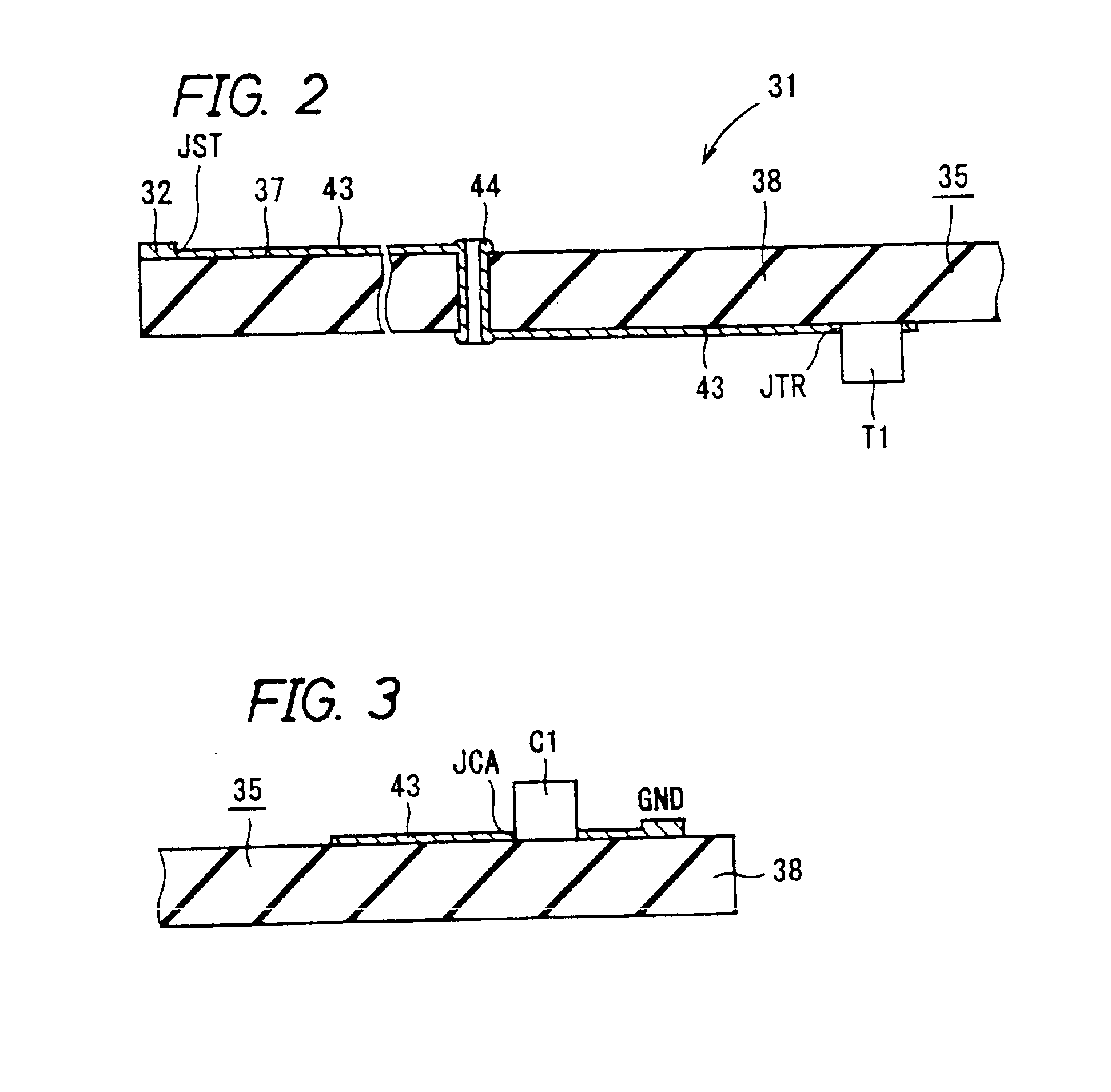
FIG. 1 is a plan view of a signal transmission circuit 31 (referred to as ‘a first signal transmission circuit’ hereafter), which is the present invention, FIG. 2 is a sectional view taken on cross-sectional line II—II of FIG. 1, FIG. 3 is a sectional view taken on cross-sectional line III—III of FIG. 1, and FIG. 4 is an equivalent circuit view of the first signal transmission circuit of FIG. 1. FIGS. 1 to 4 will be described together. The first signal transmission circuit 31 is, in electronic equipment, a circuit for transmitting signals from an input terminal section 32 to which the signals are inputted to a processing circuit section 33 in which the signals are processed. Moreover, the first signal transmission circuit 31 has a constitution for eliminating noise components of signals.

The first signal transmission circuit 31 comprises a printed wiring board 35, a transistor T1, a reference voltage source 36, a first resistor R1, a second resistor R2, a third resistor R3, and a fir...

second embodiment

Placement of conductive patterns of the printed wiring board 53 of the second signal transmission circuit 51 and placement of a circuit device onto the printed wiring board 53 are predetermined at the time of designing on the assumption that a constitution for eliminating noise components of signals is added to a constitution for signal transmission. Therefore, an intermediate transmission path 55 in the input wiring 54 (referred to as ‘second input wiring’ hereafter) of the second embodiment includes three or more conductive patterns 56 and two or more connection holes 57.

The intermediate transmission path 55 is, in the second input wiring 54, a portion from the connection point JCA between the first capacitor C1 and the second input wiring 54 to the connection point JRA between the first resistor R1 and the second input wiring 54. At least two of the conductive patterns 56 of the intermediate transmission path 55 are placed one by one on each face of the board 38. The two conducti...

third embodiment

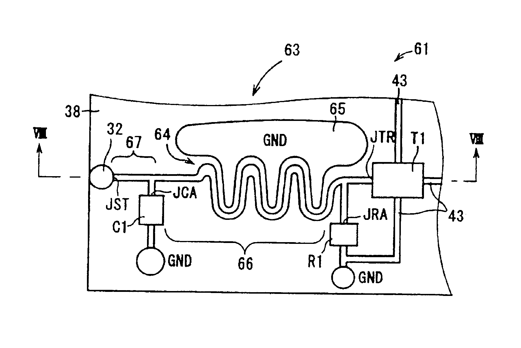
Placement of conductive patterns of the printed wiring board 63 of the third signal transmission circuit 61 and placement of a circuit device onto the printed wiring board 63 are predetermined at the time of designing on the assumption that a constitution for eliminating noise components of signals is added to a constitution for signal transmission. Therefore, an intermediate transmission path 66 in the input wiring 64 (referred to as ‘third input wiring’ hereafter) of the third embodiment is placed in the vicinity of the grounding wiring 65. The intermediate transmission path 66 is a portion of the third input wiring 64 from the connection point JCA between the first capacitor C1 and the third input wiring 64 to the connection point JRA between the first resistor R1 and the third input wiring 64.

In a case where the intermediate transmission path 66 in the third input wiring 64 exists in the vicinity of the grounding wiring 65, a parasitic capacitance c is generated between the inte...


PUM


Abstract

The respective ends of input wiring on a printed wiring board of a signal transmission circuit are connected to an input terminal section and a transistor. One terminal of a first capacitor and a first resistor are respectively connected to the input wiring. A leading-side transmission path from a connection point with the first capacitor to a connection point with the input terminal section is formed by only a conductive pattern. An intermediate transmission path from the connection point with the first capacitor to a connection point with the first resistor includes two or more through holes or via holes. The intermediate transmission path is placed near grounding wiring on the printed wiring board. When one terminal of a second capacitor is connected to the intermediate transmission path, a transmission path between the respective connection points with the two capacitors includes one or more through holes or via holes.

Description

BACKGROUND OF THE INVENTION1. Field of the InventionThe present invention relates to a signal transmission circuit for transmitting signals from an input terminal section to a processing circuit section, and an electronic equipment (device) provided with the signal transmission circuit.2. Description of the Related ArtIn related art electronic equipment, a signal transmission circuit for transmitting signals to a processing circuit section for signal processing is provided with a circuit for eliminating noise components of signals given from the outside of the electronic equipment to the electronic equipment (see, for example, Kenichi Ito, “Earth and Static Electricity”, THE NIKKAN KOGYO SHIMBUN, LTD., Jun. 30, 1980, pages 2 and 67). The noise component elimination circuit is realized by, for example, a low-pass filter constituted by a capacitor and a resistor. The noise component elimination circuit is placed right near an external terminal section.Further, in another related art c...

Claims


Application Information

Patent Timeline
Patent Type & Authority Patents(United States)
IPC IPC(8): H05K1/02H03H7/01H03H7/06H03H7/075
CPCH05K1/0231H05K1/0234H05K2201/09254H05K2201/10166H05K2201/097H05K2201/10022H05K2201/09263
Inventor KONISHI, TAKANORI
Owner FUJITSU GENERAL LTD
Why Eureka
Try Eureka