Image display device

a display device and image technology, applied in the field of display devices, can solve the problems of high-definition liquid crystal display devices, increase in scanning lines, and pixels contrast, and achieve the effects of suppressing a driving voltage waveform, suppressing a cost increase, and preventing erroneous writing

Inactive Publication Date: 2005-03-01
SHARP KK
View PDF4 Cites 31 Cited by
  • Summary
  • Abstract
  • Description
  • Claims
  • Application Information

AI Technical Summary

Benefits of technology

It is an object of the present invention to provide an image display device capable of preventing erroneous writing while (i) suppressing an incr...

Problems solved by technology

Drawbacks to the simple matrix liquid crystal display device are as follows: (i) reduction in contrast of pixels on display, which is caused by an increase in the number of scanning lines, which causes an effective voltage to be applied to a liquid crystal at each point of intersection of the scanning lines to gradually decrease toward a tip, that is not suitable for a high-definition liquid crystal display device; and (ii) low response speed.
Such a change of the scanning voltage waveform into a dull waveform raises a problem such that it causes deviation in the ON/OFF timing of the TFT 1051 at the both input and termination ends of the scanning lines, and an application of a signal voltage at the following stage earlier than the switch of the TFT 1051 to an OFF state at the termination end causes a signal of the following stage to be written into a pixel, thereby occurring erroneous writing.
However, this method has a problem such that enlarging the width of a line increases the ratio of the area of a wiring portion within a pixel, thereby reducing the number of apertures through which light is transmitted.
First, as shown in FIG. 11, a method for staggering the respective ON timings of a scanning voltage and a signal voltage has a problem as follows: since offset is allowe...

Method used


Image

  • Image display device
  • Image display device
  • Image display device

Examples


Embodiment Construction

The following will explain one embodiment of the present invention with reference to drawings.

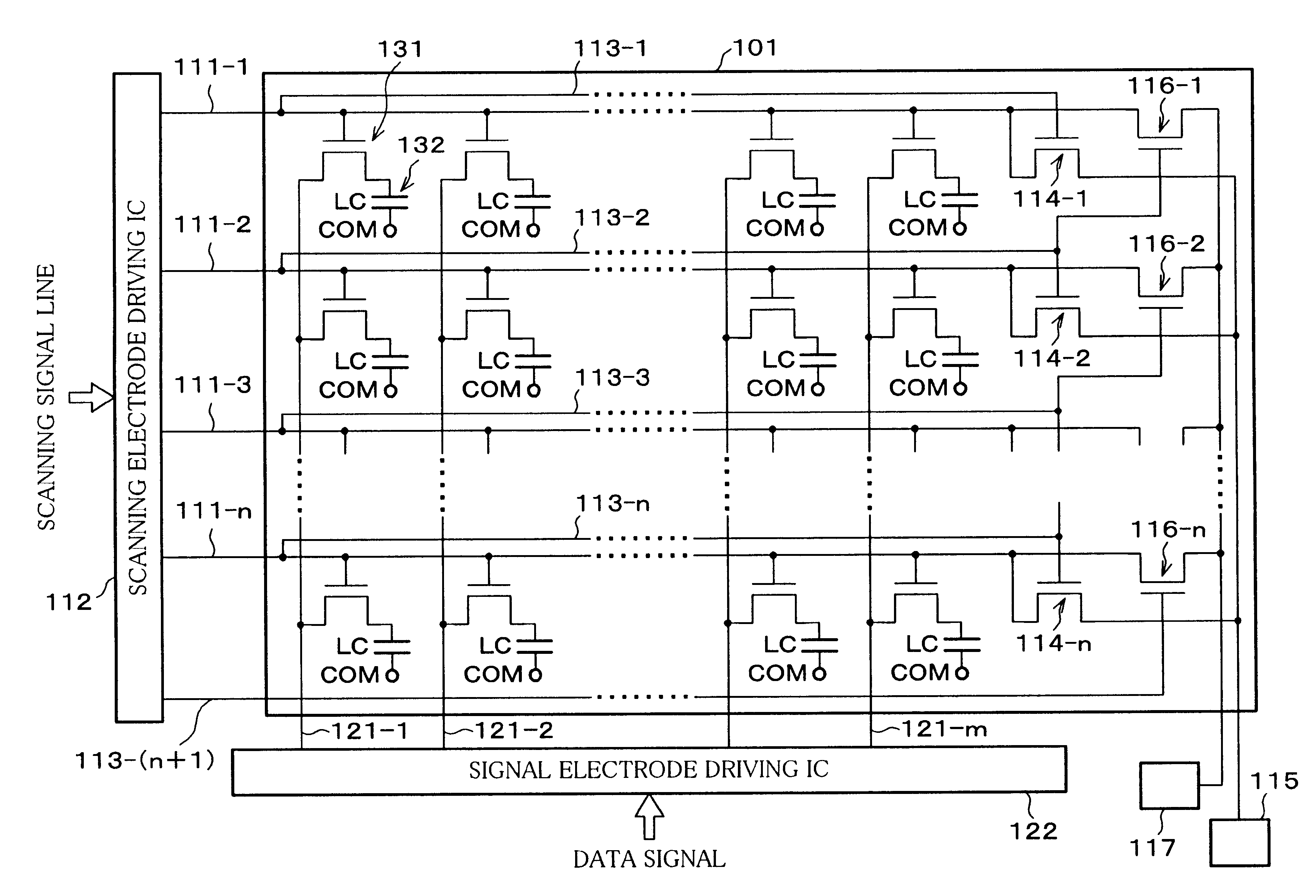
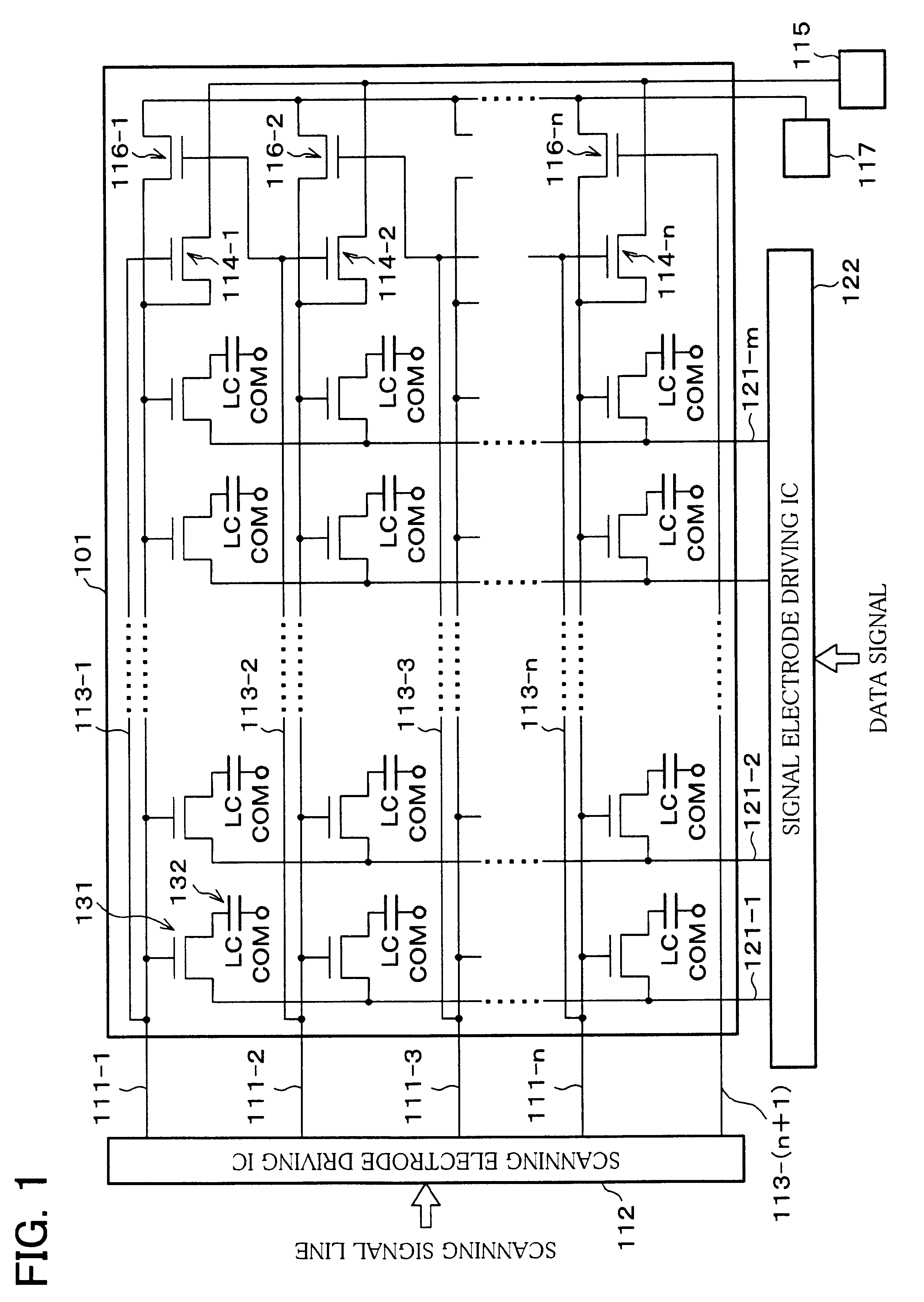
FIG. 1 shows a circuit configuration of a liquid crystal display device according to the present embodiment. As shown in FIG. 1, the liquid crystal display device includes, within a display panel 101, scanning lines 111-1 to 111-n and signal lines 121-1 to 121-m disposed in a lattice state, and a liquid crystal pixel 132 connected at a crossing point of a scanning electrode and a signal electrode via a pixel TFT 131. Further, with respect to the scanning lines 111-1 to 111-n and the signal lines 121-1 to 121-m are respectively connected a scanning electrode driving IC 112 and a signal electrode driving IC 122.

Further, on one side of the display panel 101 closer to the scanning electrode driving IC 112, the scanning lines 111-1 to 111-n are respectively connected with scanning auxiliary lines 113-1 to 113-n having smaller wiring resistance and allowing less growth of a dull signal (smaller s...


PUM


Abstract

On a termination side of each scanning line is provided a charging switching element and a discharging switching element in parallel with each other, the charging switching element having a gate electrode which is connected with one end of a scanning auxiliary line, the other end of which is connected to a scanning line of the same stage, the discharging switching element having a gate electrode which is connected with one end of a scanning auxiliary line, the other end of which is connected to a scanning line of the following stage. Further, the charging switching element has a source/drain electrode which is connected to a scanning line and a selected state scanning driving voltage power source, whereas the discharging switching element has a source/drain electrode which is connected to a scanning line and the non-selected state scanning driving voltage power source, thereby allowing an image display device of the present invention to suppress the dull waveform of a driving voltage at both rise and fall, and prevent erroneous writing without reducing effective writing time.

Description

FIELD OF THE INVENTIONThe present invention relates to a display device capable of display such as liquid crystal display and EL (Electro-Luminescence) display, and in particular to a display device driven by an active matrix.BACKGROUND OF THE INVENTIONFIGS. 7(a) and 7(b) show schematic cross sectional views respectively showing configurations and operation of a liquid crystal display device.As shown in FIG. 7(a), the liquid crystal display device has an arrangement in which on one side of a glass substrate 1001 is formed an electrode 1002, on one side of a glass substrate 1011 is formed an electrode 1012, and further, on the electrodes 1002 and 1012 are respectively printed alignment materials on which alignment films 1003 and 1013 are respectively formed. After the formation of the alignment films 1003 and 1013, rubbing is applied to the alignment film 1003 in a direction parallel to a paper surface and the alignment film 1013 in a direction perpendicular to the paper surface. Fur...

Claims


Application Information

Patent Timeline
IPC IPC(8): G09G3/36G02F1/133G02F1/1343G09F9/30G09G3/20
CPCG09G3/3677G09G2320/0223G02F1/133
Inventor TAKEUCHI, MASANORINAGASHIMA, NOBUYOSHIKONDO, NAOFUMIMITSUMOTO, KAZUYORI
Owner SHARP KK
Why Eureka
Try Eureka