Method for masking ringing in DDR SDRAM

a ringing phenomenon and masking technology, applied in the field of masking a ringing phenomenon in a ddr sdram, can solve the problems of inability to adjust the dsfb>2/b> signal, inability to prevent the write fail from occurring, and increasing the discrepancy resulting from write failur

Active Publication Date: 2005-03-01
SK HYNIX INC
View PDF21 Cites 27 Cited by
  • Summary
  • Abstract
  • Description
  • Claims
  • Application Information

AI Technical Summary

Benefits of technology

In order to achieve the above object, according to one aspect of the present invention, there is provided a method for masking a ringing phenomenon in a DDR SDRAM comprising: in a write mode, generating a first and a second synchronizing signal by means of a DQS signal inputted from an exterior circuit, in order to synchronize input data; latching data in odd sequences from among the inputted data, which are sequentially inputted, at a rising edge of the first synchronizing signal, and latching data in even sequences from among the inputted data, which are sequentially inputted, at a rising edge of the second synchronizing signal; aligning the data in odd sequences and the data in even sequences at a falling edge of the DQS signal so that the odd and even sequenced data has the same synchronized timing; and blocking activation of the second synchronizing signal by means of a first control signal, the first control signal being synchronized with the falling edge of the last valid DQS signal that is normally inputted, so as to enable the blocking st

Problems solved by technology

However, with the recent developments in memory cell technology, discrepancies resulting from write fail are increasing due to the number of memory modules built into the mother-boards or due to increases in clock frequency, etc.
As a result, a discrepancy may result because the last two data D2 and D3 stored in a latch are replaced with the invalid data, and are then transmitted to a global input/output bus line.
In use of the above described conventional methods, the following problem may occur.
That is, under the condition in which tD is larger than (tDG+tDA), the conventional circuit for masking the ringing can

Method used


Image

  • Method for masking ringing in DDR SDRAM
  • Method for masking ringing in DDR SDRAM
  • Method for masking ringing in DDR SDRAM

Examples


Embodiment Construction

Hereinafter, a preferred embodiment of the present invention will be described with reference to the accompanying drawings.

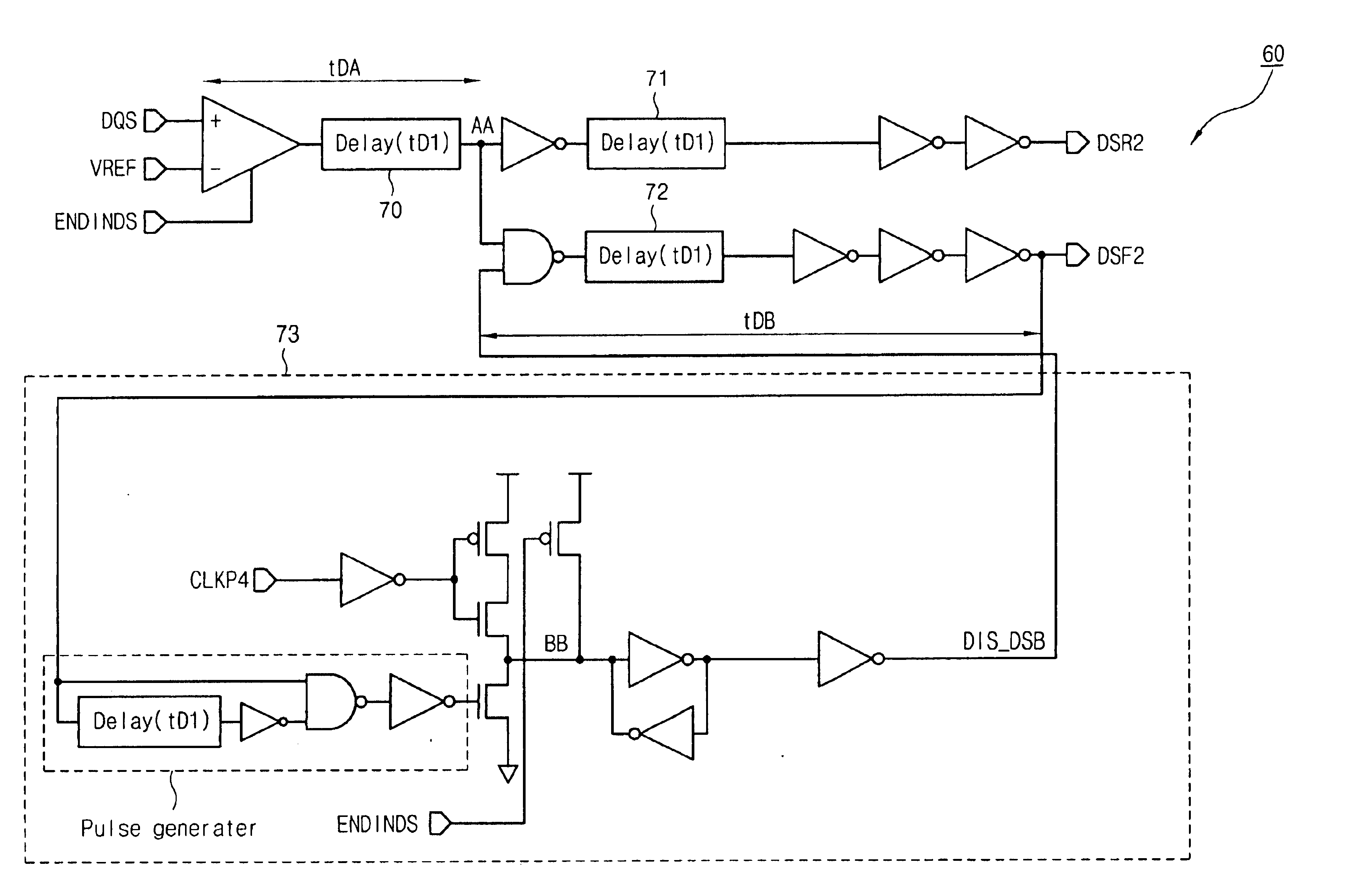
FIG. 7 is a block diagram illustrating a DQS input buffer 60, which includes a circuit for masking a write fail due to a ringing, according to the present invention. The DQS input buffer 60 may be utilized within the circuit shown in FIG. 2 to enable the masking of the ringing phenomenon.

As shown in FIG. 7, the construction of the circuit according to the present invention has essentially the same construction as that of the circuit shown in FIG. 4, except for the construction of the circuit 73 for masking the write fail due to the ringing phenomenon.

Further, the circuit 73 shown in FIG. 7 for masking the write fail due to the ringing phenomenon is different from the circuit in FIG. 4, in that the circuit 73 does not have the delay block, as shown in the construction of FIG. 4 for causing the delay time tDC.

First, the operation of the circuit 73 for masking the ...


PUM


Abstract

A method for masking a ringing in a DDR SDRAM comprises in a write mode, generating first and second synchronizing signals by means of a DQS signal inputted from an exterior circuit, in order to synchronize input data, latching data in odd sequences from among the inputted data, which are sequentially inputted, at a rising edge of the first synchronizing signal, and latching data in even sequences from among the data, which are sequentially inputted, at a rising edge of the second synchronizing signal, aligning the data in odd sequences and the data in even sequences at a falling edge of the DQS signal so that the odd and even sequenced data has the same synchronized timing, and blocking activation of the second synchronizing signal by means of a first control signal, the a first control signal being synchronized with the falling edge of the last valid DQS signal that is normally inputted, so as to enable the blocking step and thereby masking the ringing phenomenon. In the method for masking the ringing phenomenon, the point at which the DIS_DSB signal is enabled in a low state is synchronized with the last falling edge of the normal DQS signal, and therefore the DSF2 signal is disabled.

Description

BACKGROUND OF THE INVENTION1. Field of the InventionThe present invention relates generally to a method for masking a ringing phenomenon in a DDR SDRAM, and more particularly to a method for masking a ringing phenomenon in a DDR SDRAM which can mask a write fail due to a ringing phenomenon of a DQS signal applied in a write operation in the DDR SDRAM.2. Description of the Background ArtIn general, when a double data rate (DDR) SDRAM performs a write operation, the DDR SDRAM latches data at a rising and a falling edge of a DQS signal, and thus operates twice as fast as the frequency of a clock signal CLK. That is, it operates at double data rate (hereinafter, referred to as a DDR). However, such a DDR operation is performed in only an input / output buffer, and the operation in the DDR SDRAM is performed at one-clock intervals as in the operation of an SDRAM.Further, in order to realize such a DDR operation, during operation of the DDR SDRAM, two DQS signals DSR2 and DSF2 are generated...

Claims


Application Information

Patent Timeline
IPC IPC(8): G11C8/00G11C11/40G11C7/10
CPCG11C7/1093G11C7/1078G11C11/40
Inventor SHIN, BEOM JU
Owner SK HYNIX INC
Why Eureka
Try Eureka