Semiconductor device testing apparatus and semiconductor device manufacturing method using it

a technology of semiconductor devices and testing apparatus, which is applied in the direction of individual semiconductor device testing, semiconductor/solid-state device testing/measurement, instruments, etc., can solve the problems of difficult to secure the area where each wiring line is to be formed, and achieve the effect of avoiding problems such as beam breakage and local concentration of stress in the beam

Inactive Publication Date: 2005-03-08
RENESAS ELECTRONICS CORP
View PDF6 Cites 6 Cited by
  • Summary
  • Abstract
  • Description
  • Claims
  • Application Information

AI Technical Summary

Benefits of technology

An object of the present invention is to provide a semiconductor device testing apparatus that can be miniaturized while the strength of beams is kept at a required level and that hence can accommodate many probes. It is also an object of the present invention to provide a semiconductor device manufacturing method using such a testing apparatus.
Where each wiring line is formed on the surface of the associated double-support beam where the associated probe is formed, so as to extend at both sides of the probe on a front face where the probe is placed on the beam, especially, so as to extend to the two support portions at both ends of the beam, the beam always has the same sectional shape taken in the width direction at any arbitrary position in the longitudinal direction of the beam. As a result, the second moment of area that is determined by the shapes of the beam and the wiring line is made constant. This prevents a problem that the curvature of the beam varies locally when the beam is brought into contact with a subject body, and is thereby bent by a prescribed amount.
As a result, local concentration of stress in the beams is prevented and problems such as breakage of a beam can be avoided.
Where each wiring line is formed on the surface of the associated cantilever where the associated probe is formed, so as to extend at least to the support portion of the associated cantilever, the neutral axis is shifted, and the distance between the neutral axis and a portion of the support portion of the cantilever where the tensile stress is strong becomes smaller.
Since the stress is reduced, a semiconductor device testing apparatus can be realized that can be miniaturized while the strength of cantilevers is kept at a required level and that, hence, can accommodate many probes.

Problems solved by technology

Notwithstanding their intention to provide improved probe testers, the above prior art structures have the following problems.
In this prior art structure, if the intention is to increase the number of probes from the current number, it becomes difficult to secure the area where each wiring line is to be formed.

Method used


Image

  • Semiconductor device testing apparatus and semiconductor device manufacturing method using it
  • Semiconductor device testing apparatus and semiconductor device manufacturing method using it
  • Semiconductor device testing apparatus and semiconductor device manufacturing method using it

Examples


second embodiment

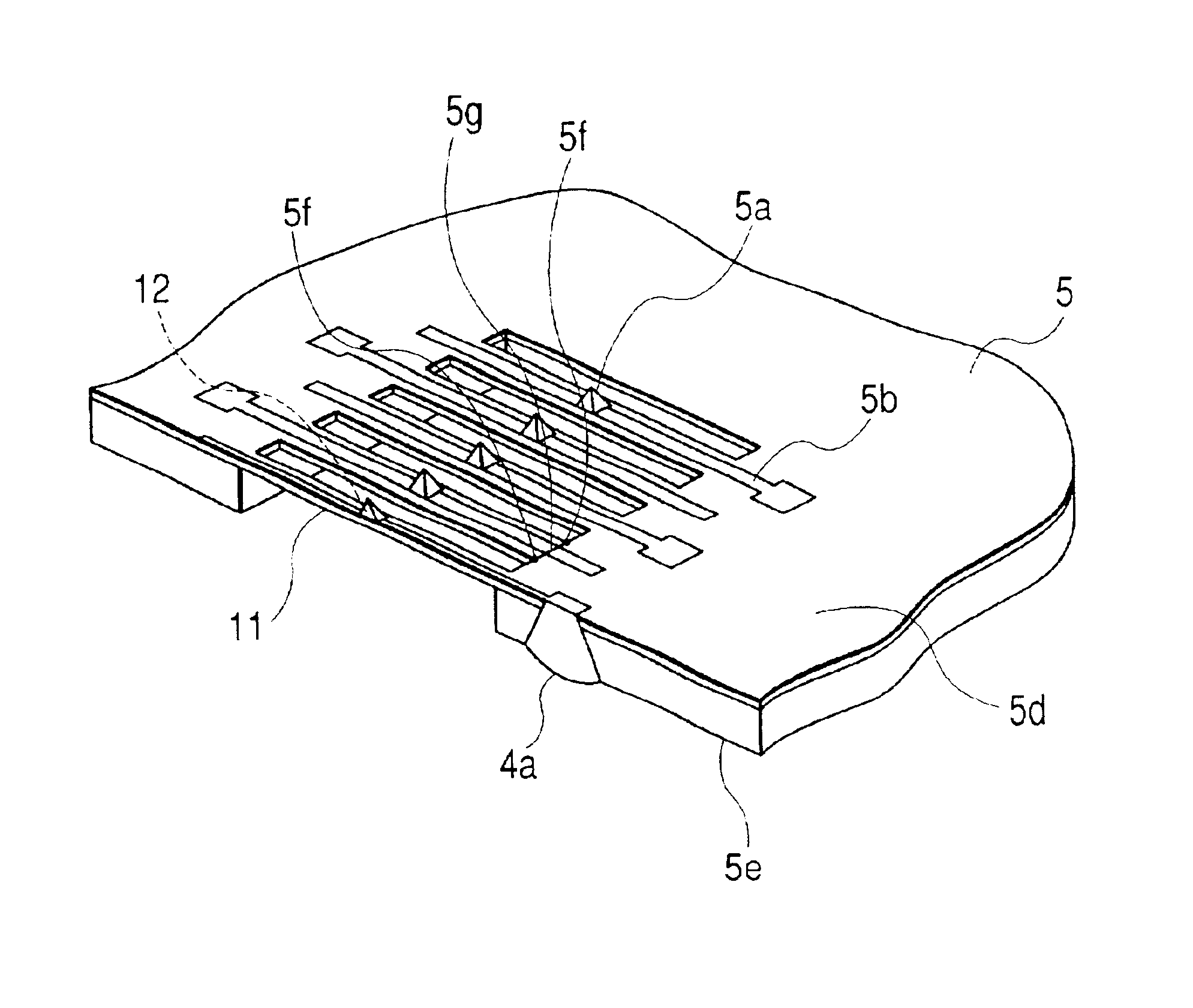
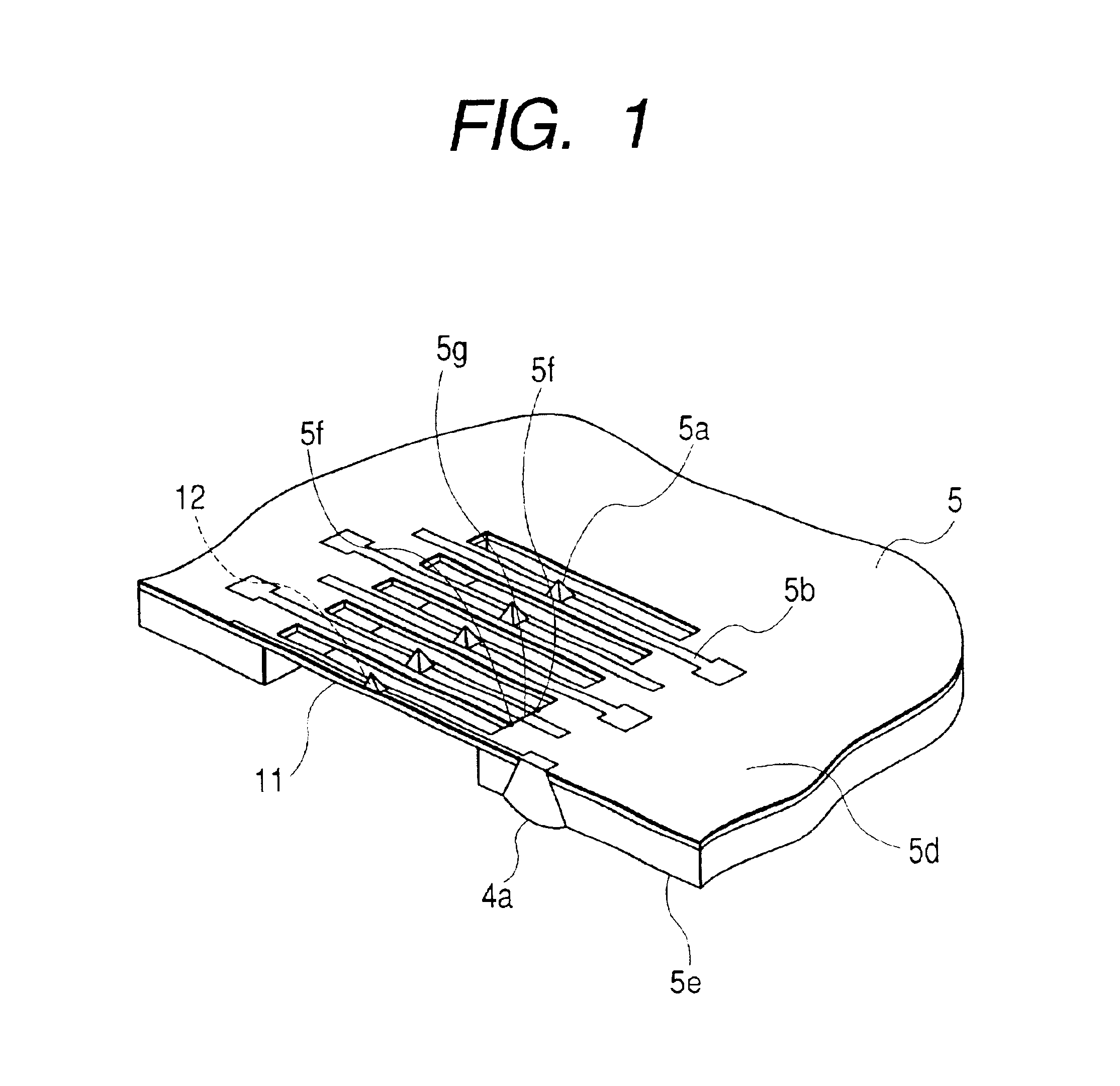
Next, the invention will be described with reference to FIGS. 3 and 4.

FIG. 3 is an enlarged perspective view of the main part of a semiconductor device testing apparatus according to the second embodiment of the invention, that is, a perspective view of the main part of a substrate 5 that is part of a probe structure, and in which probes are formed. FIG. 4 is a sectional view of part of the probe formation substrate 5 of FIG. 3 taken along the longitudinal direction of a beam 11.

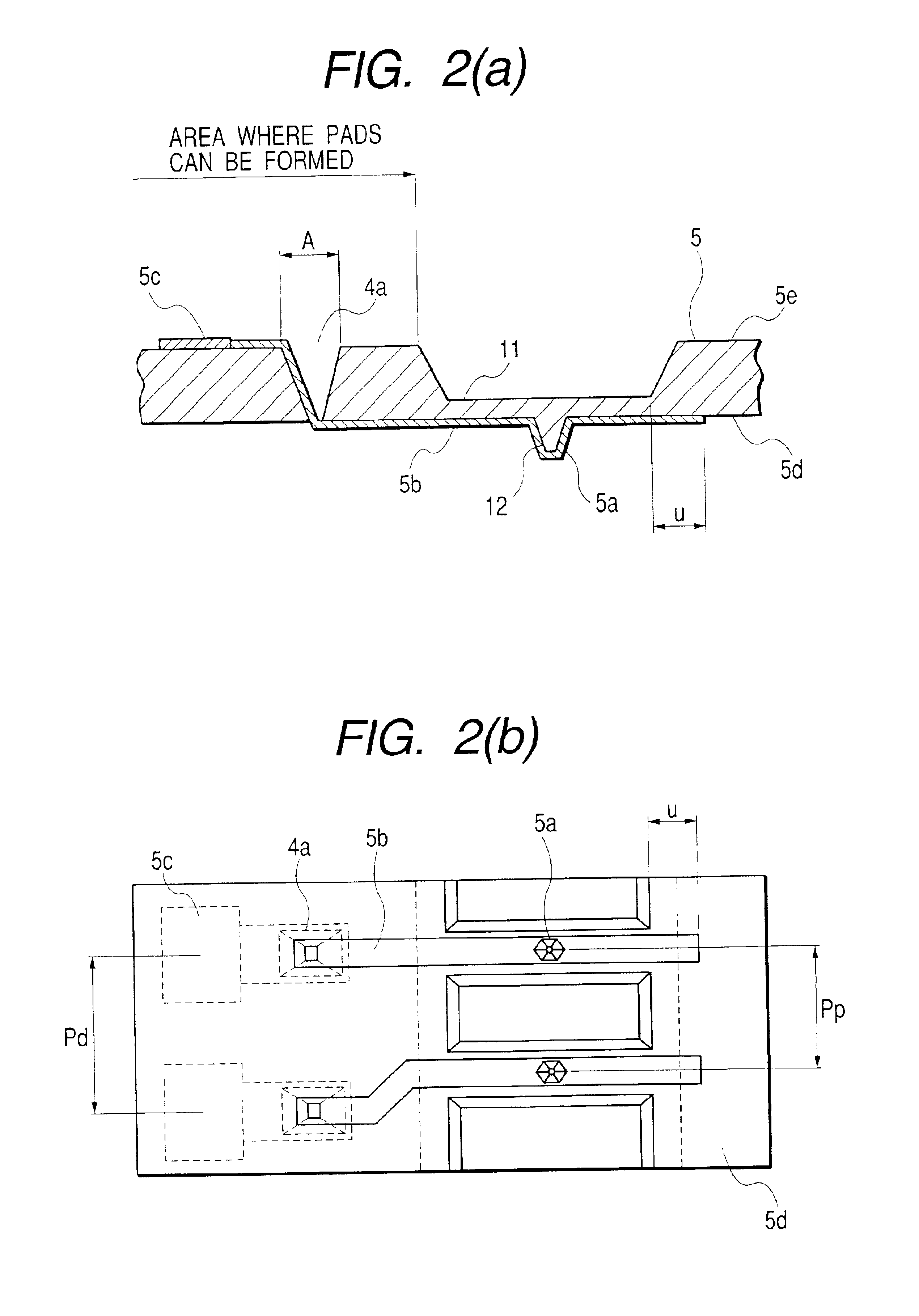
In the second embodiment of the invention, the beams 11 are cantilevers rather than double-support beams as employed in the first embodiment. Part of each line 5b extends on a side surface 111 of the beam 11, that is, a surface connected to a surface 5d where probes 5a are formed, and is connected to a secondary electrode 5c. In the probe formation surface 5d, each line 5b extends to the base portion of the beam 11 and forms an overlap having a value u in the same manner as in the first embodiment.

A first ef...

third embodiment

the invention will be described with reference to FIGS. 5 and 6.

FIG. 5 is an enlarged perspective view of the main part of a semiconductor device testing apparatus according to the third embodiment of the invention, that is, a perspective view of the main part of a substrate 5 that is part of a probe structure, and in which probes are formed. FIG. 6 is a sectional view of part of the probe formation substrate 5 of FIG. 5, taken along the longitudinal direction of a beam 11.

In the third embodiment of the invention, unlike the case of the second embodiment, each line 5b is formed along the minimum path that is necessary to secure the electrical characteristics required. To attain the same effects as in the second embodiment, a film 13 is formed on the bottom surface of each beam 11 separately from the line 5b.

In the above-described second embodiment, each line 5b itself is used to improve the bending characteristic of the beam 11. However, this design increases the formation area of ...


PUM


Abstract

Since each wiring line is formed on one surface of the associated beam at a prescribed width over the entire length of the beam, the beam has the same sectional shape taken in the width direction at any point along an arbitrary longitudinal direction of the beam. As a result, the second moment of area, which is determined by the shapes of the beam and the wiring line, is uniform. This prevents a problem of the curvature of a beam varying locally when the beam is bent by a prescribed amount due to contact of the probe with a pad of a subject body. This, in turn, prevents local concentration of stress in the beams and thereby prevents breakage of the beam. Therefore, the probe structure can be miniaturized while the strength of the beams is kept at a required level, whereby a semiconductor device testing apparatus capable of accommodating many probes can be realized.

Description

BACKGROUND OF THE INVENTION1. Field of the InventionThe present invention relates to a semiconductor device testing apparatus and a semiconductor device manufacturing method using it. In particular, the invention relates to a testing apparatus capable of increasing the efficiency of a test process for a semiconductor device, and to a semiconductor manufacturing method using such a testing apparatus.2. Description of the Related ArtFirst, a conventional semiconductor device manufacturing method will be described below.A semiconductor manufacturing process is generally divided into what is called a pre-process in which many LSIs are formed on each wafer and various test processes are executed on the LSIs, and an assembling process in which each LSI is completed into a final product form. Such a typical manufacturing process will be described with reference to FIG. 15.FIG. 15 is a flowchart outlining a general manufacturing method of a semiconductor device. The manufacturing method inc...

Claims


Application Information

Patent Timeline
IPC IPC(8): G01R3/00G01R1/073G01R31/28H01L21/66
CPCG01R3/00G01R1/07357H01L22/00
Inventor KOHNO, RYUJIMIURA, HIDEOKANAMARU, MASATOSHISHIMIZU, HIROYABAN, NAOTO
Owner RENESAS ELECTRONICS CORP
Why Eureka
Try Eureka