Liquid crystal display and manufacturing method thereof

a technology of liquid crystal display and manufacturing method, which is applied in the field of liquid crystal display, can solve the problems of more difficult control of a small cell gap than a large cell gap, and achieve the effect of high display quality

Inactive Publication Date: 2005-03-08
SHARP KK
View PDF33 Cites 50 Cited by
  • Summary
  • Abstract
  • Description
  • Claims
  • Application Information

AI Technical Summary

Benefits of technology

A principal objective of the present invention is to provide a liquid crystal display that has two or more different, stable

Problems solved by technology

Generally, it is more difficult to contro

Method used


Image

  • Liquid crystal display and manufacturing method thereof
  • Liquid crystal display and manufacturing method thereof
  • Liquid crystal display and manufacturing method thereof

Examples


embodiment 1

[Embodiment 1]

The following will describe an embodiment of the present invention in reference to FIG. 1 through FIG. 6.

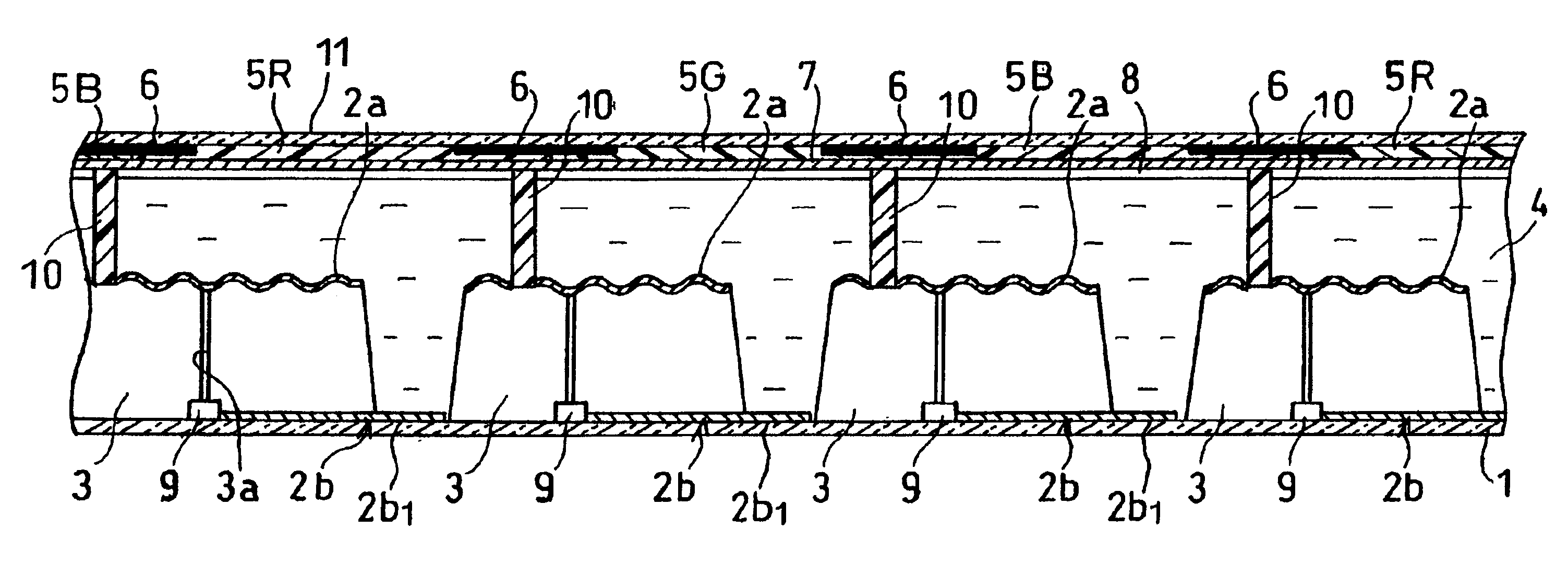
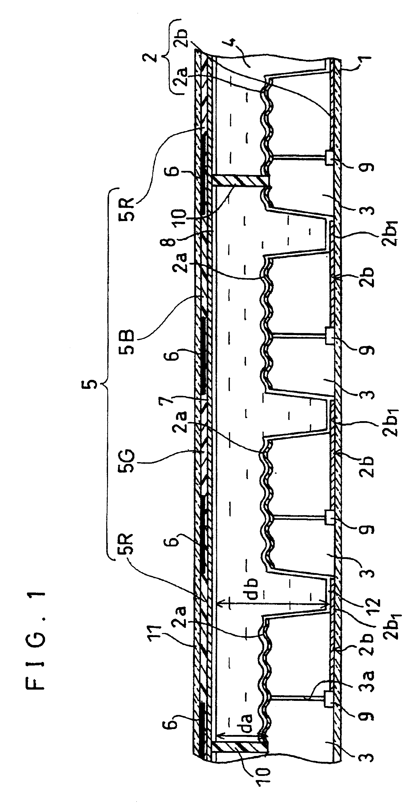
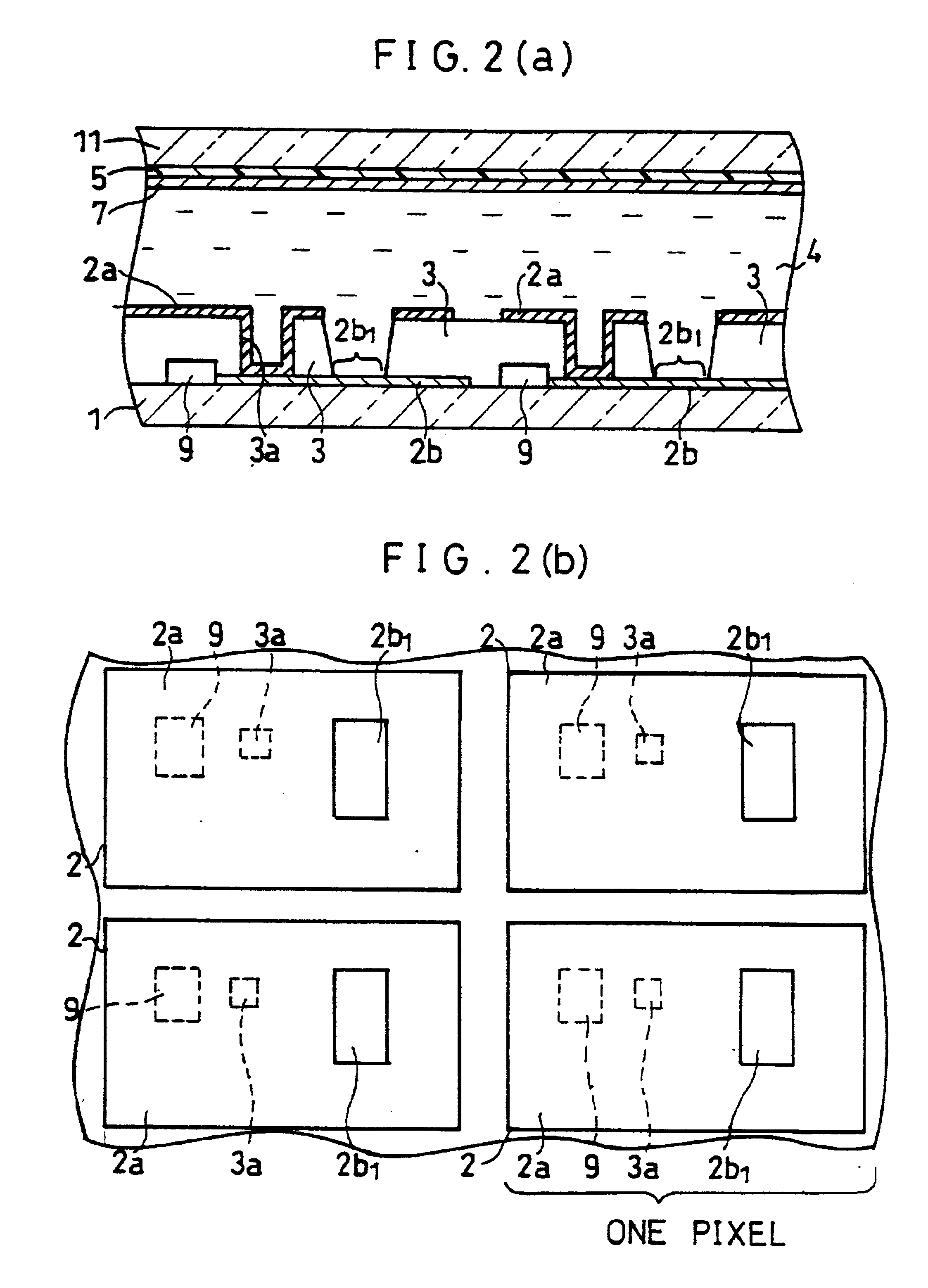
FIG. 1 is a cross-sectional view showing a structure of the major part of a liquid crystal display. As shown in FIG. 1, the liquid crystal display in accordance with the present embodiment contains, between a substrate 1 and an opposite substrate 11, pixel electrodes 2, an interlayer insulation layer 3, a liquid crystal layer 4, color filters 5, black matrices (BMs) 6, a transparent electrode 7, an alignment layer 8, thin film transistors (TFTs) 9, columnar spacers 10, and another alignment layer 12.

On the substrate 1 are located the TFTs 9, the pixel electrodes 2, the interlayer insulation layer 3, and the alignment layer 12. On the opposite substrate 11 are deposited the color filters 5 with the BMs 6; the transparent electrode 7, and the alignment layer 8 in this order. The substrate 1 and the opposite substrate 11 are located opposite each other with the columna...

embodiment 2

[Embodiment 2]

The following will describe another embodiment of the present invention in reference to FIGS. 7, 8. Here, for convenience, members of the present embodiment that have the same arrangement and function as members of the previous embodiment, and that are mentioned in that embodiment are indicated by the same reference numerals and description thereof is omitted.

FIG. 7 is a cross-sectional view of the major part of a liquid crystal display in accordance with an embodiment of the present invention. FIG. 8 is an enlarged explanatory drawing showing the major part of an opposite substrate 11 of FIG. 7. The substrate 1 disposed opposite the opposite substrate 11 with an intervening liquid crystal layer 4 is identical in the present embodiment and in embodiment 1 as shown in FIG. 7.

As shown in FIG. 8. the opposite substrate 11 here has color filters 5 with BMs 6, columnar spacers 10, and a transparent electrode 7 on the opposite substrate 11 as in embodiment 1. Each blue filte...


PUM


Abstract

A liquid crystal display has spacers for maintaining a liquid crystal layer and a cell gap between a substrate and an opposite substrate and also has regions either within a single pixel or over two or more pixels. The spacers are of columnar shape elongated from the substrate to the opposite substrate or the other way round, and the columnar spacers are provided in regions in which the liquid crystal layer is thinnest among those regions in which the liquid crystal layer varies in thickness. The structure makes the liquid crystal display having two or more different cell gaps to stably maintain those cell gaps and produces good quality displays.

Description

FIELD OF THE INVENTIONThe present invention relates to liquid crystal displays in general and those liquid crystal displays with a liquid crystal layer that varies in thickness from one pixel to another or within one pixel in particular, and further relates to manufacturing methods of those liquid crystal displays.BACKGROUND OF THE INVENTIONLiquid crystal displays are thin and low power-consuming and for these reasons are used extensively for example, in office automation equipment, such as word processor devices and personal computers; personal digital assistants, such as electronic note pads; and VTRs with a built-in camera and a liquid crystal monitor.Liquid crystal panels do not emit light as CRTs (Cathode Ray Tubes) and EL (electroluminescense) displays. Instead, some liquid crystal panels include in the back thereof a section containing a so-called backlight, which is a fluorescent tube, and produces a display by controlling the transmission / interruption of the light emitted b...

Claims


Application Information

Patent Timeline
IPC IPC(8): G02F1/13G02F1/1339G02F1/1335G02F1/1333G02B5/20
CPCG02F1/13394G02F1/133555G02F1/1339G02F1/1335
Inventor FUJIMORI, KOICHINARUTAKI, YOZOSHINOMIYA, TOKIHIKO
Owner SHARP KK
Why Eureka
Try Eureka