
Single mask via method and device

a single mask and mask technology, applied in the field of three-dimensional integrated circuit fabrication, can solve the problems of increasing chip cost, increasing chip area, and reducing chip yield, so as to minimize the amount of substrate used and maximize the interconnect density

Active Publication Date: 2005-03-15
INVENSAS BONDING TECH INC
View PDF7 Cites 191 Cited by
  • Summary
  • Abstract
  • Description
  • Claims
  • Application Information

AI Technical Summary

Benefits of technology

It is another object of the present invention to avoid patterning a mask in a recess.
Another object of the present invention is to maximize the interconnect density between two stacked ICs.
Another object of the present invention is to minimize the amount of substrate used to form an interconnection between two stacked ICs.

Problems solved by technology

However, in spite of this increased transistor density, a continual demand in increased IC complexity and functionality has resulted in a continued increase in IC chip area.
This increase in chip area results in a reduction in chip yield and, correspondingly, increased chip cost.
This increase in mask levels and IC area also result in a reduction in yield, and correspondingly, increased chip cost.
The cost of the interconnect portion of this approach is directly related to the number of photolithography masking levels required to etch vias and form electrical interconnects.
The die substrate can not, in general, be totally removed due to the location of transistors in the substrate.
This results in a patterning over a non-planar structure that limits the scaling of the structure to very small feature size that is desirable to achieve the highest interconnection density and consumes the least possible silicon substrate where functional transistors would otherwise reside.

Method used


Image

  • Single mask via method and device
  • Single mask via method and device
  • Single mask via method and device

Examples


first embodiment

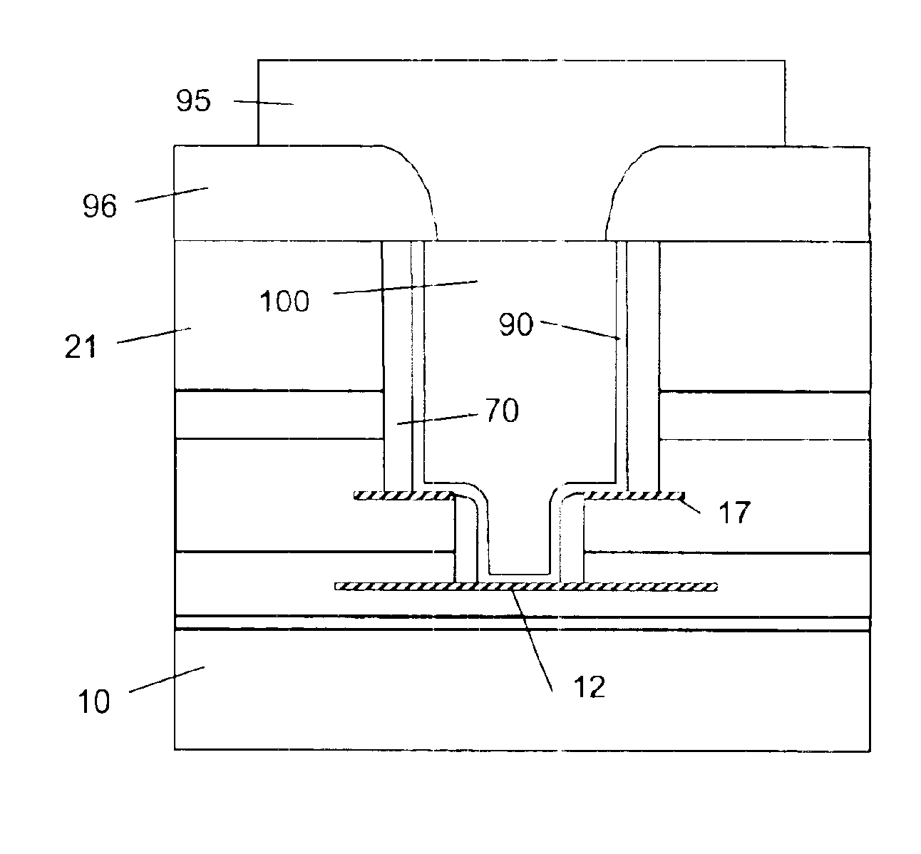
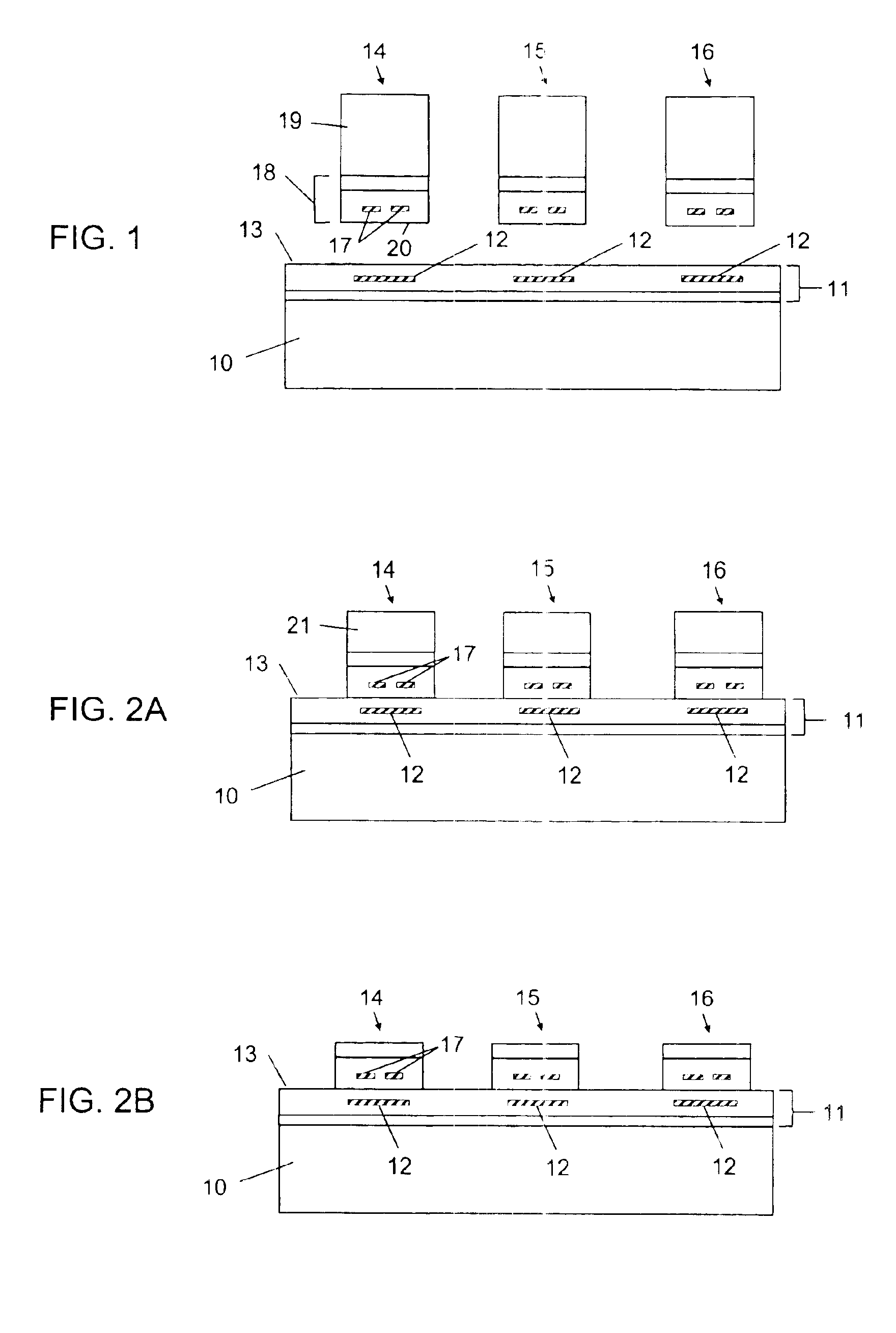
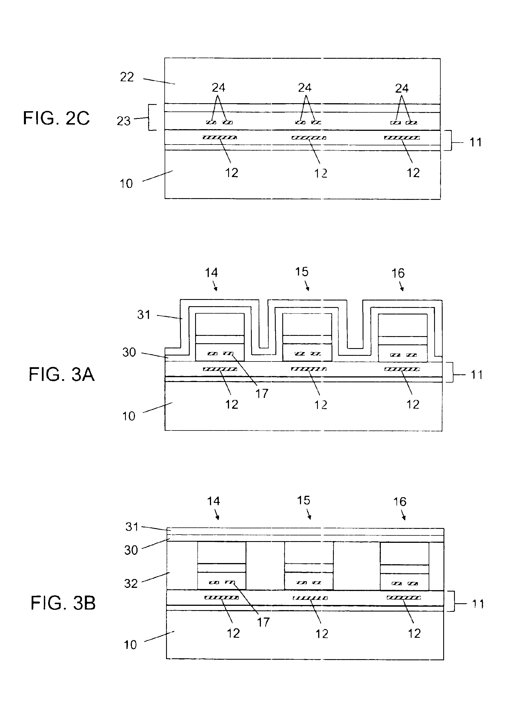
Referring now to the drawings, in particular FIG. 1, the method according to the invention will be described. It is noted here that the drawings are not drawn to scale but are drawn to illustrate the concepts of the invention.

Substrate 10 includes a device region 11 having contact structures 12. Substrate 10 may be made of a number of materials, such as semiconductor material or insulating material, depending on the desired application. Typically, substrate 10 is made of silicon or III-V materials. Contact structures 12 are typically metal pads or interconnect structures making contact to device or circuit structures (not shown) formed in substrate 10. Substrate 10 may also contain an integrated circuit to which the contact structures 12 are connected, and substrate 10 may be a module containing only contact structures. For example, substrate 10 may be a module for interconnecting structures bonded to substrate 10, or bringing out connections for packaging or integration with other ...


PUM


Abstract

A method of connecting elements such as semiconductor devices and a device having connected elements such as semiconductor devices. A first element having a first contact structure is bonded to a second element having a second contact structure. A single mask is used to form a via in the first element to expose the first contact and the second contact. The first contact structure is used as a mask to expose the second contact structure. A contact member is formed in contact with the first and second contact structures. The first contact structure may have an aperture or gap through which the first and second contact structures are connected. A back surface of the first contact structure may be exposed by the etching.

Description

BACKGROUND OF THE INVENTION1. Field of the InventionThe present invention relates to the field of three-dimensional integrated circuits and more particularly to the fabrication of three-dimensional integrated circuits using direct wafer bonding.2. Description of the Related ArtSemiconductor integrated circuits (ICs) are typically fabricated into and on the surface of a silicon wafer resulting in an IC area that must increase as the size of the IC increases. Continual improvement in reducing the size of transistors in ICs, commonly referred to as Moore's Law, has allowed a substantial increase in the number of transistors in a given IC area. However, in spite of this increased transistor density, a continual demand in increased IC complexity and functionality has resulted in a continued increase in IC chip area. This increase in chip area results in a reduction in chip yield and, correspondingly, increased chip cost.Another trend in IC fabrication has been to increase the number of d...

Claims


Application Information

Patent Timeline
Patent Type & Authority Patents(United States)
IPC IPC(8): H01L23/52H01L21/70H01L23/538H01L21/768H01L23/48H01L21/98H01L25/065
CPCH01L21/76898H01L23/481H01L24/83H01L24/94H01L25/0657H01L25/50H01L2924/0132H01L2924/014H01L2924/01023H01L2924/01005H01L2924/14H01L2924/10329H01L2924/01078H01L25/0655H01L2221/68354H01L2224/83894H01L2224/94H01L2225/06517H01L2225/06524H01L2225/06541H01L2924/01013H01L2924/01029H01L2924/01033H01L2924/01042H01L2924/01049H01L2924/01074H01L2924/01077H01L2224/83H01L2924/01015H01L2924/01031H01L21/76805H01L23/48H01L23/538
Inventor ENQUIST, PAUL M.
Owner INVENSAS BONDING TECH INC
Features
  • Generate Ideas
  • Intellectual Property
  • Life Sciences
  • Materials
  • Tech Scout
  • Unparalleled Data Quality
  • Higher Quality Content
  • 60% Fewer Hallucinations
Learn More