Method for developing a photoresist pattern

a technology of resist and pattern, applied in the direction of liquid processing circulation, coating, photographic processes, etc., can solve the problems of resist line collapse, resist line mechanical stability decline, resist line collapse, etc., and achieve the effect of reducing post-development defects

Active Publication Date: 2005-03-29
ASML NETHERLANDS BV
View PDF11 Cites 13 Cited by
  • Summary
  • Abstract
  • Description
  • Claims
  • Application Information

AI Technical Summary

Benefits of technology

The above objective is achieved in accordance with the present invention by providing a novel me...

Problems solved by technology

Unfortunately, as the demands of the microelectronics industry require smaller feature sizes, the line width defined by the resist is likewise becoming smaller.
With increasing aspect ratio, the mechanical stability of the resist lines decreases and post-development defect...

Method used


Image

  • Method for developing a photoresist pattern
  • Method for developing a photoresist pattern
  • Method for developing a photoresist pattern

Examples


Embodiment Construction

In the following description, in order to facilitate a thorough understanding of the invention and for purposes of explanation and not limitation, specific details are set forth, such as the process steps to reduce post-development defects or a particular geometry of the mixing nozzle. However, it should be understood that the invention may be practiced in other embodiments that depart from these specific details.

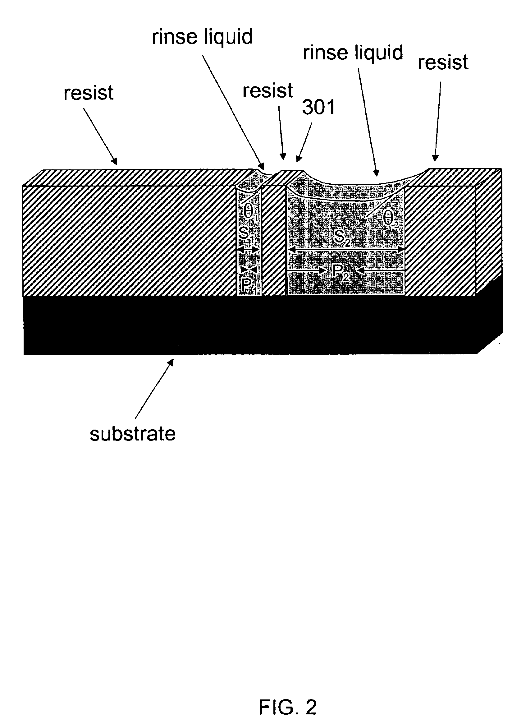
In the present document, the term “photoresist pattern” is used to encompass a latent image formed on the photoresist layer, after exposure, and a developed photoresist pattern.

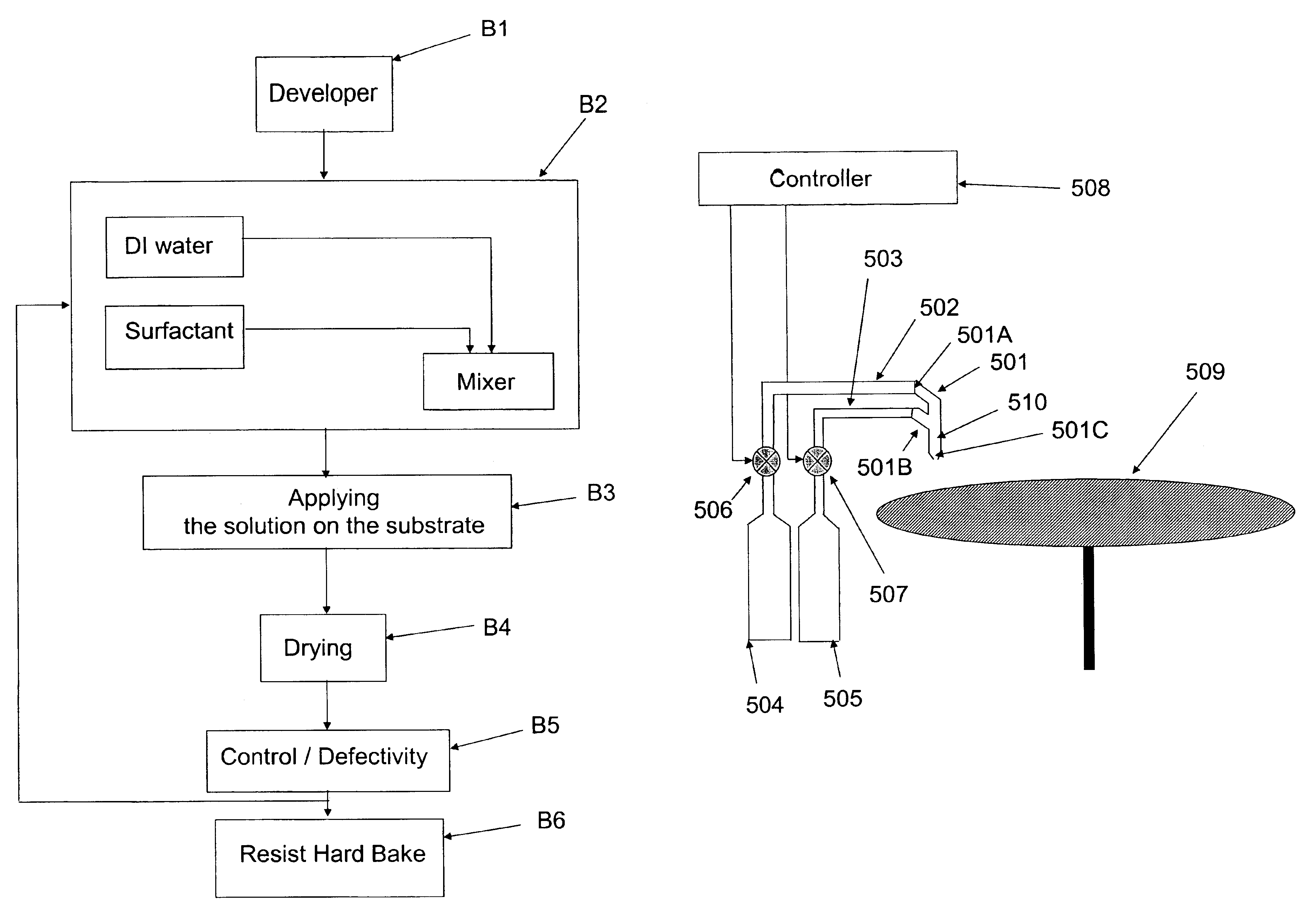
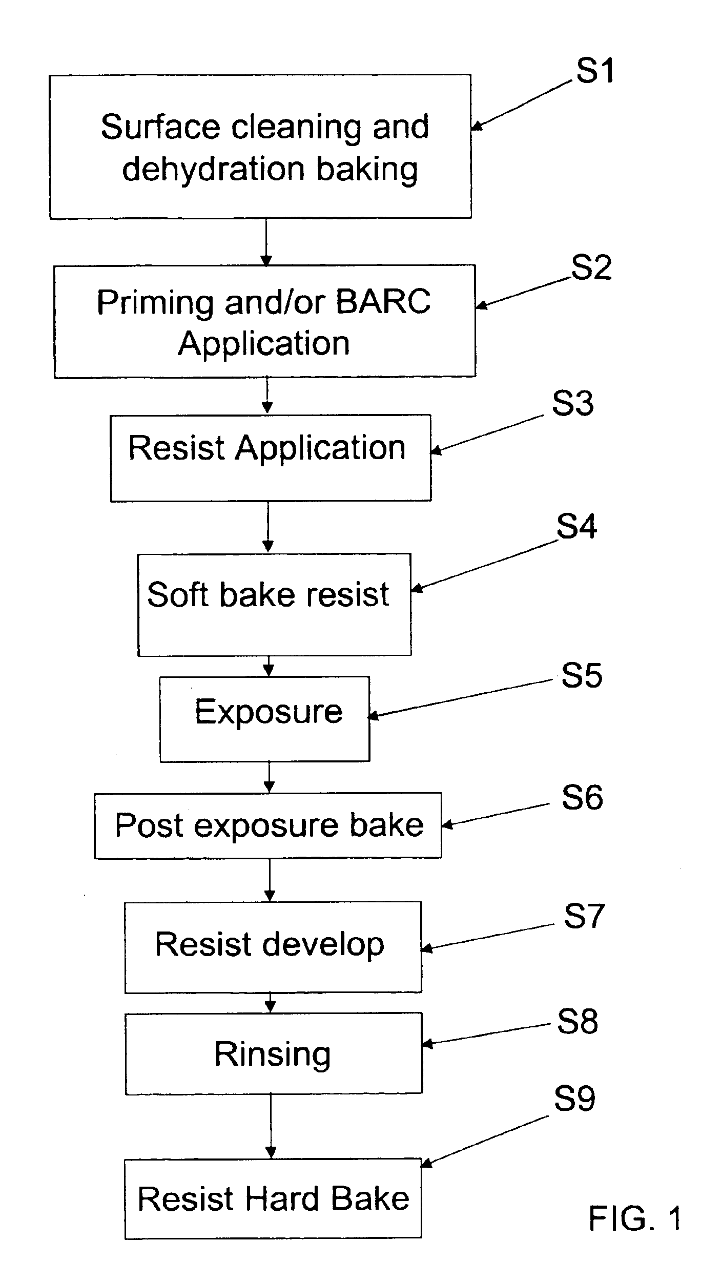
Basic steps that may be used in the photoresist process for the fabrication of an IC device according to one embodiment of the invention are illustrated in FIG. 1.

The method begins at (S1) where a surface cleaning and a dehydration baking are carried out to prepare the surface for photoresist application, though as one of ordinary skill in the art will appreciate, this step is not always necessary. T...


PUM


Abstract

The present invention relates to a method for developing a photoresist pattern. The method consists of mixing a concentrated chemical solution with a solvent to obtain a diluted chemical solution of a predetermined concentration. In this method, the mixing is done in a fabrication facility where the substrates are processed. The diluted chemical solution is then applied onto the photoresist pattern. Analysis of the pattern is then carried out to detect any defects or pattern collapse on the substrate. In the event that defects and/or pattern collapse occur, the predetermined concentration is adjusted to reduce the phenomenon.

Description

BACKGROUND OF THE INVENTION1. Field of the InventionThis invention relates to a method for developing a photoresist pattern, and more particularly to a method for developing a photoresist pattern wherein post-development defects are reduced.2. Description of Related ArtPhotolithography is an essential driver of the microelectronics industry. The ability to continually shrink designs to the point where sub-wavelength feature resolution is now routine, has allowed the industry to continue the trend toward higher device densities. To maintain this rate of development and to accomplish high device packing density, it has become necessary to incorporate sophisticated photolithographic processes.Photolithography is the production of a three-dimensional image based on the patterned exposure to light and subsequent development of a light-sensitive photoresist on the wafer surface. Broadly stated, a radiation-sensitive photoresist is applied to a substrate such as a wafer and then an image e...

Claims


Application Information

Patent Timeline
IPC IPC(8): G03D5/00G03F7/30G03F7/40
CPCG03F7/3021G03F7/40
Inventor PAXTON, THEODORE A.DAVIS, TODD
Owner ASML NETHERLANDS BV
Why Eureka
Try Eureka